To improve yield, find the design-sensitive defects
By Matt Knowles – Mentor, A Siemens Business
Whether you are trying to accelerate yield ramp on a new process or boost your margins on established nodes, you need a way to find and fix yield limiters. Diagnosis-driven yield analysis, DDYA, is a methodology for digital semiconductor devices that pulls in production test results, volume scan diagnosis, and statistical analysis to identify the cause of yield loss prior to failure analysis. This methodology can reduce the time to finding the root cause of a failure by 75-90%, and identify systematic yield limiters that would otherwise never be found.
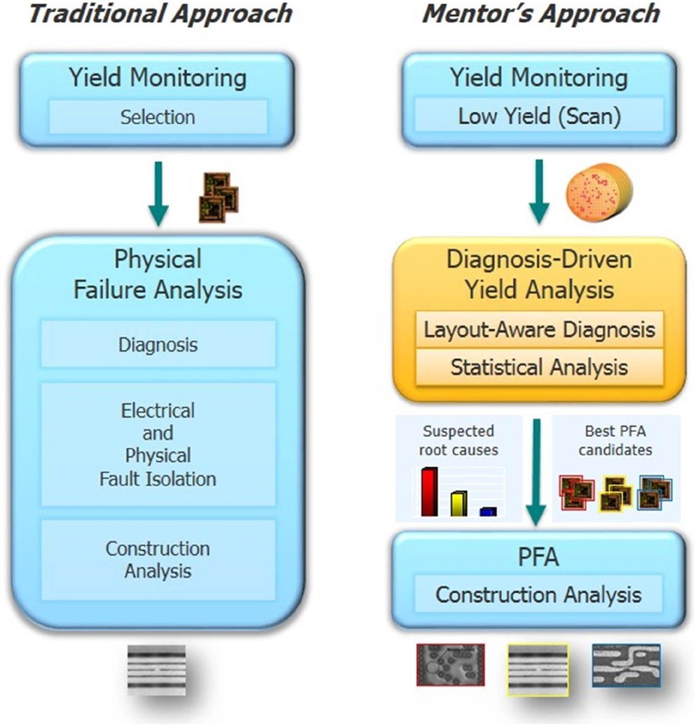 DDYA is a step above traditional scan diagnosis. Scan diagnosis uses a design description, scan test patterns, and fail data from a tester to identify “suspects”, i.e. the most likely defects that caused the failures during digital test. The main goal of the traditional flow is to localize the defect that causes failures on a specific die. But, for yield analysis, the location of the defect isn’t sufficient to determine whether defects in different locations on multiple die are caused by the same mechanism or not.
DDYA doesn’t just use diagnosis for defect localization, it can determine the underlying root causes and the best physical failure analysis (PFA) candidates in a batch such as a wafer or lot of failing devices. DDYA leverages layout information like cell type, via type, layer, and critical area. With DDYA, you can also find defects that are internal to the cells with transistor-level (Cell-Aware) fault models derived from analog simulation.
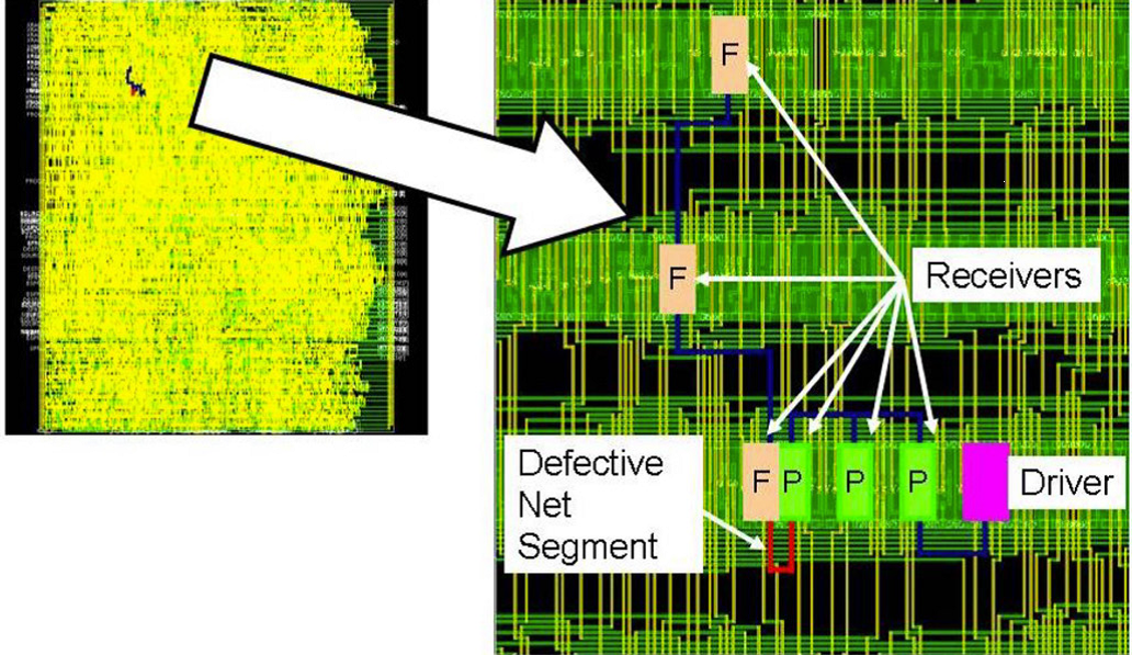
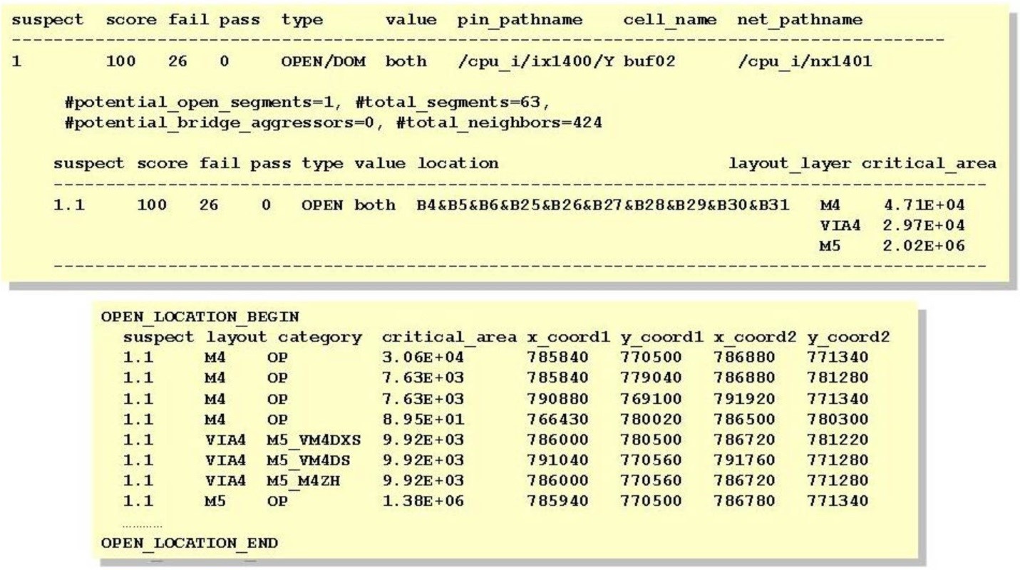
Because DDYA is layout-aware, it locates a suspect defect much more precisely than traditional scan diagnosis. For example, the following figure shows a net that was found to have an open defect with scan diagnosis. With DDYA, the open is narrowed down to a segment of a net by analyzing all the receivers in a multi-fanout-out net.
Of particular interest when doing yield analysis is how the layout information is leveraged in the reports output by the tool. In the report shown below for a failing die, you can see the physical location down to x, y, and layer along with logic location and classification. In this example, the suspected defect is an open in a net segment containing metal4, metal5, and three different types of vias. When similar information is generated for other failing die, this information can be analyzed and processed to determine which characteristics are of particular interest.
Tessent Diagnosis provides a comprehensive set of diagnosis capabilities that provides more than 50 different attributes for each failure. These attributes, which range from failing scan chain and patterns to defect classification and affected standard cells, provide the foundation for the statistical analysis performed by Tessent YieldInsight.
For details, download the whitepaper Overcoming Systematic Yield Limiters with Diagnosis-Driven Yield Analysis
The Tessent diagnosis-driven yield analysis capabilities reduce the cycle time to root cause of yield loss by 75-90%. This translates into faster yield ramp for new processes and boosts in profit from mature processes.