Transistor-Level Defect Diagnosis
By Geir Eide, Mentor Graphics
Need to diagnose silicon failures faster and with more accuracy? Try the new cell-aware diagnosis to pinpoint the source of failures within standard cells.
Each new semiconductor process node represents exciting opportunities for suppliers of design, manufacturing, test, and failure analysis solutions. A new process means new challenges to solve, and hopefully more money to be made. On the flip side, whenever solutions that address these new challenges are presented, we seldom hear how useful these are to more mature process nodes. One technology that has received a lot of attention recently is “cell-aware” test and failure diagnosis. With more defects inside cells at leading-edge nodes, cell-aware test, which deterministically targets defect locations inside cells, and cell-aware diagnosis, which can identify defects at the transistor level, are natural solutions.
The reality is that the vast majority of semiconductor devices are manufactured at technologies that are two, three, or more nodes behind the leading edge. How useful is cell-aware technology at these more mature nodes? In this article, we focus on cell-aware diagnosis, which identifies the location and type of cell-internal or transistor-level defects. Rather than identifying a standard cell instance as the source of the failure, cell-aware diagnosis can identify a much smaller portion of the cell.
One situation where cell-aware diagnosis is valuable no matter the process node is in the context of large, complex cells such as adders, multipliers, and multi-bit sequential elements. Even when a defect is known to be within a cell, finding defects in such a complex cell in physical failure analysis (PFA) can be daunting. Determining whether such a defect is systematic or yield limiting typically requires the examination of a large number of failing die, which can take several months. So, while many, or even most defects can be found using traditional methods, not having a way to tackle defects in complex cells is a bit like driving without insurance. You will be just fine – for a while.
Cell-aware diagnosis short-cuts the lengthy investigation process by pinpointing a small subsection of the suspected cell. Figure 1 shows the results of a case study published at the 2016 European Test Symposium (ETS) that compared cell-aware diagnosis results to PFA results for a 160nm automotive design [1]. After cell-aware diagnosis determined a suspect defect location to be a bridge between two nets inside the cell, the actual defect, a poly-contact short, was found in PFA after delayering to the polysilicon level. This is a defect mechanism that would be missed in traditional diagnosis.
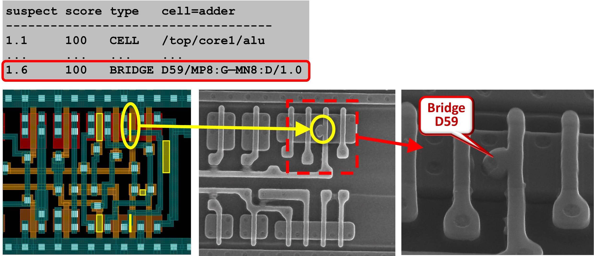
Figure 1: Cell-aware diagnosis narrows down the location of a failure at the transistor level. Image from P. Maxwell, et.al, “Cell-Aware Diagnosis: Defective Inmates Exposed in their Cells”, European Test Symposium (ETS) 2016.
What makes cell-aware diagnosis possible is a unique fault model that is created by analog simulation for all physical defects extracted from the library cell layout. The layout information for each defect is stored for the diagnosis process and the critical area and the related defect probability of each potential bridge and open defect is analyzed. A high probability is reached when the distance of the adjacent nets is just 1 technology length and the length of the bridging area is, for example, 10 or more technology lengths. A low probability is present when the bridging length is just 1 technology length and the distance of the adjacent objects is, for instance, 10 times or more the technology length. An analog simulator is then used to simulate each potential defect against an exhaustive set of stimuli to determine if there are sets of cell inputs that produce an output sufficiently different than the defect-free result.
These models are used during diagnosis, along with the design description, tester failure data, and the test patterns. Cell-aware diagnosis works for any ATPG pattern type, such as stuck-at, transition delay, and cell-aware. This means that the overall data collection and diagnosis flow remains the same compared to a traditional flow. The diagnosis reports list the best matching suspects with the layout information after considering both interconnect suspects and cell internal suspects. The comprehensive layout picture from the proposed covering both interconnect defects and cell-internal defects is helpful for guiding the PFA process and performing yield learning.
A typical cell-aware diagnosis result is shown in Figure 2. In this case, two cell-internal suspects are called out, both bridges, between internal nets in the cell. These represent a very small portion of the overall cell, even in this case which is a relatively simple NAND2 gate.
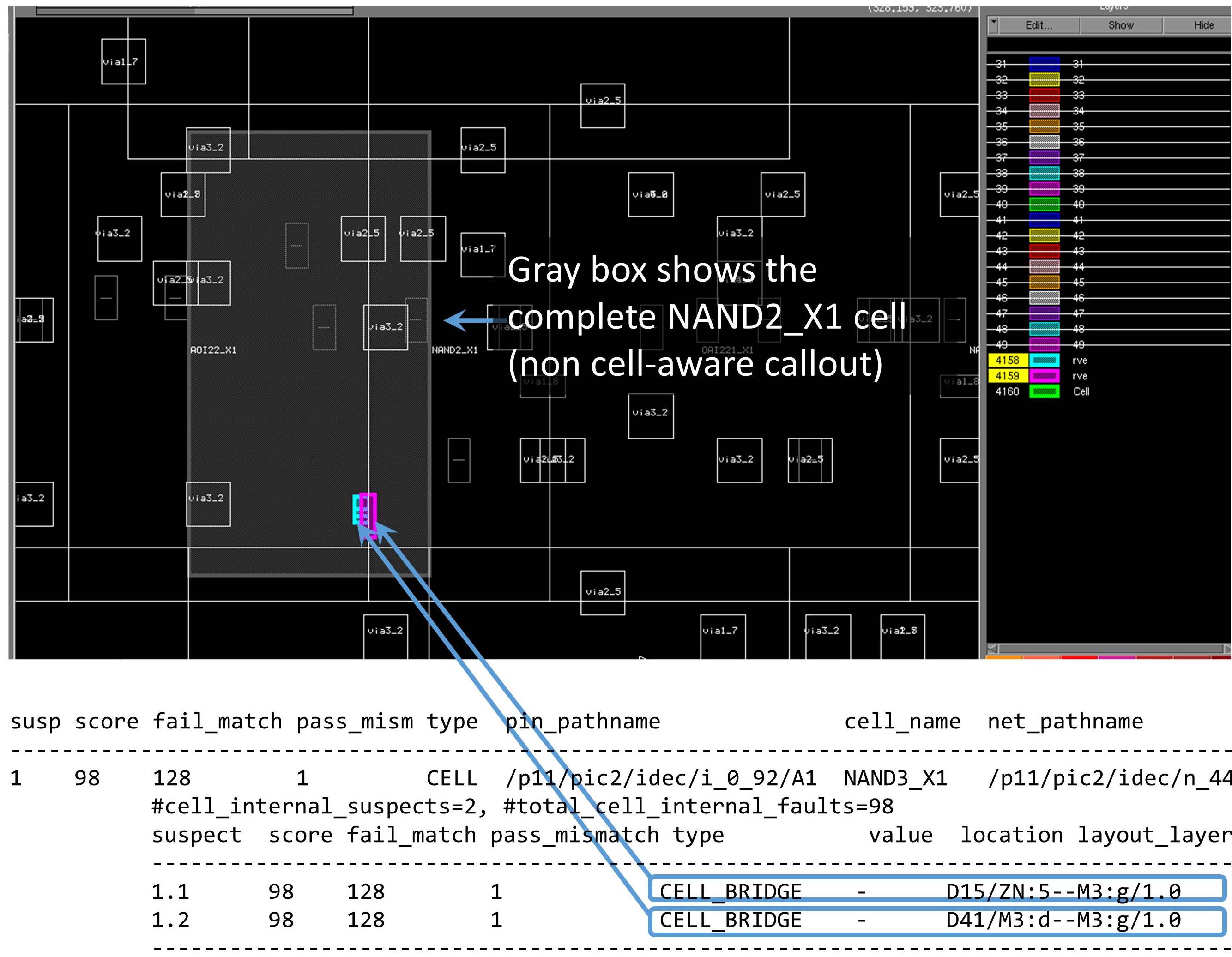
Figure 2: Cell-aware diagnosis result finding two bridge suspects with a standard cell.
Cell-aware diagnosis has been shown to improve diagnosis resolution for cell-internal defects by up to 70X on a complex cell, and by over 10X on average. Cell-aware diagnosis is enabled by a layout-justified cell-aware fault model, which is generated once per library. Cell-aware diagnosis improves results for single-part diagnosis scenarios such as customer return analysis as well as volume diagnosis applications like yield analysis, even for designs that are manufactured on mature nodes.
References:
[1] P. Maxwell, et.al, “Cell-Aware Diagnosis: Defective Inmates Exposed in their Cells”, European Test Symposium (ETS) 2016, https://www.mentor.com/products/silicon-yield/ieee_conference_papers/
Author
Geir Eide is the product marketing director for the Silicon Learning product line in the Silicon Test Solutions group at Mentor Graphics. His focus is on diagnosis, yield analysis, and silicon debug.

Liked this article? Then try this –
Blog: Take scan test out of the critical path
This article was originally published on www.semiengineering.com