Scan ATPG and compression are beating Moore’s law
By Ron Press, Mentor Graphics
Why hasn’t IC test become a bottleneck in creating ever more advanced semiconductors? In this article, Ron Press tells the story of how scan ATPG has stayed a step ahead of Moore’s Law.
Moore’s law has been the standard reference for semiconductor scaling. It roughly says that semiconductor design sizes, fueled by technology improvements, double every two years. Consequentially, the complexity of designing and fabricating semiconductors continues to grow, requiring increasing efforts and larger design teams. It was the increase in complexity and development costs that led to the development of electronic design automation (EDA).
Doubling design sizes every two years is an exponential growth rate. But when designs double in size, the effort it takes to design and test them often exceed the 2x factor. Sequential logic adds a complexity factor that is also an additional exponential growth rate. For example, a 16-bit state machine is more than twice as complex as an 8-bit state machine. The growth in volume of test data is directly related to increased cost of test, so there is a strong business case for controlling test data volume.
Fortunately for semiconductor test, scan technology was proposed in 1973 and was ready for use by 1979. Scan provides a structural test methodology by dividing the complex functional logic into many small combinational parts that are easy for automation to test. With scan test, the complex nature of the design and the actual function of the design is removed from the problem of automated test pattern generation (ATPG).
As design process technologies continued to scale down and design sizes continued to go up, test times were controlled for several years through continuous improvements in ATPG algorithms.
Yet, the demands for test compression as Moore’s law continued unabated threatened to outpace the available technologies. Eventually, a more dramatic solution was necessary, and embedded compression technology was introduced. With fabrication process technologies below 180 nm (and certainly below 130 nm), designers found that existing test patterns, such as static suck-at tests, were no longer enough to thoroughly test a circuit. Between 180 nm to 130 nm, for example, the population of timing-based defects grew up to 20x, forcing the industry to adopt the at-speed scan test methodology referred to as transition fault testing.[1]
One of the earliest embedded compression technologies was Illinois scan, a technique that involves connecting many internal scan chains to a common scan channel, which could produce about 11x improvement in test time. By 2004, the adoption of transition patterns was driving a demand for even more compression, and the next big improvement, on-chip compression and decompression, was ready to meet the industry’s new test challenges. Embedded compression quickly became essential for controlling potential huge increases in test cost.
Recently, even more testing has been added with the use of cell-aware test, which targets defects at the transistor level, inside standard cells. Cell-aware test is being rapidly adopted because it significantly improves defect detection. However, it also adds to the test volume problem that compression technologies are always trying to control.
Figure 1 illustrates the incremental advances in compression technology, normalizing a design in 2000 and showing the exponential design scaling of Moore’s law. Notice that around 2004, transition patterns were adopted by industry, which added another 1.5x on top of the traditional stuck-at pattern size.
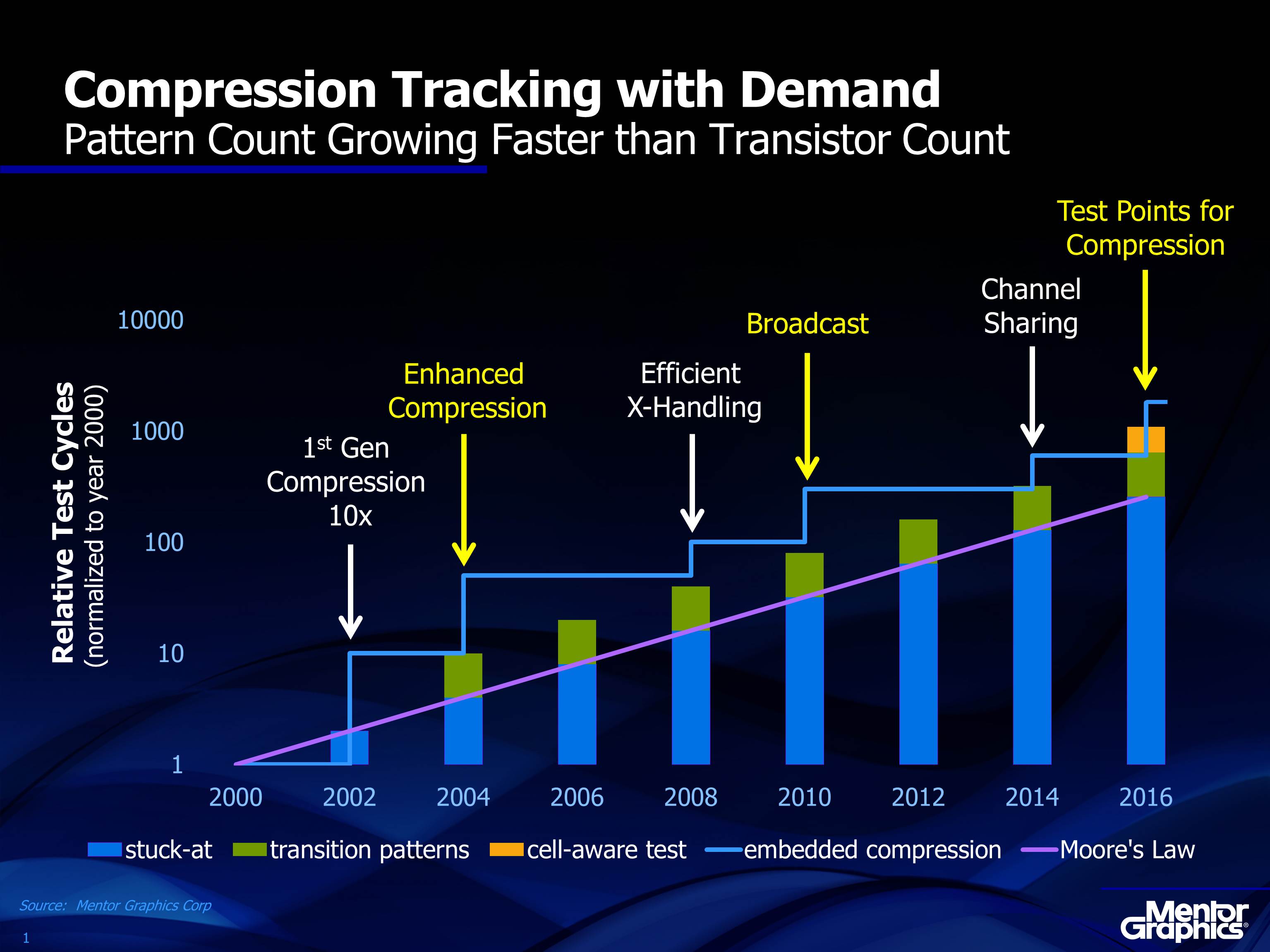
Figure 1. Incremental improvements in compression algorithms and technology
Source: Keynote delivered by Walden Rhines at the 2016 International Test Conference
Some of the design scaling we’ve seen over the last decade has been due to more and more integration of functions into single devices, often with duplicate blocks. In response, compression technology introduced better handling of broadcasting to duplicate blocks. Then in 2014, compression technology added channel sharing, where multiple non-identical blocks can share the majority of tester channels in parallel. In 2016, along with the quick adoption of cell-aware test, which can increase pattern size by 70%, we have the latest innovation in compression in a new type of test point that specifically reduces compression ATPG pattern count. Previous test-point approaches might provide an incremental improvement, but the new test points using advanced analysis and efficient algorithms are proven to provide 3-4x additional compression. This helps offset the recent additional pattern growth with cell-aware test.[2] [3]
The EDA industry and its technology partners have done a great job keeping up with design scaling and pattern type demands, improving algorithms, and inventing whole new approaches. As shown in Figure 1, the cumulative compression compared to the capabilities in 2000 is over 1,000x better. What will be the next great test innovation to enable further scaling? Further innovations are in the works, but there remains some low-hanging fruit in improving test flows and methodologies to better align with the way SoCs are designed. In many companies’ test flow, the DFT work is done late in the design cycle, after all the blocks of the SoC are done. Rather than waiting until the entire SoC design is finished before starting DFT, why not complete DFT and ATPG as each block is ready? A hierarchical DFT methodology, which breaks big designs into separate blocks for ATPG and then reuses and retargets the test to the full design later, often provides an additional 2x or better improvement in test compression. This is not a new methodology, but the EDA industry has developed new technologies to make it efficient. With new test software, it is easy to directly reuse patterns created at the block level. Block-level patterns are retargeted to the top level independent of the top-level design variations, automatically adjusting for pipelines and merging independently-created block patterns together where desired.
In the face of numerous potential crises in testing IC over the last 40 years, the EDA industry has always pulled off advances in test flows and technologies to keep pace with design scaling. The pipeline for inventions in test technology is not slowing down, so don’t worry about silicon test being the downfall of semiconductor progress in the future.
References
[1] G. Aldrich, B. Cory, “Improving Test Quality and Reducing Escapes,” Proceedings of the Fabless Forum, Fabless Semiconductor Association, 2003, pp. 34-35.
[2] J. Rajski, M. Kassab, N. Mukherjee, N. Tamarapalli, “Embedded Deterministic Test for Low-Cost Manufacturing,” IEEE Design & Test of Computers, 2003.
[3] C. Acero, F. Hapke, et al., “On New Test Points for Compact Cell-Aware Tests,” IEEE Design & Test, 2016.
Author
Ron Press is the technical marketing director of Silicon Test Solutions products at Mentor Graphics Corp.

Liked this article? Then try this –
Blog: Take Scan Test Out of the Critical Path
This article was originally published on www.evalutationengineering.com