Experiment vs. Simulation, Part 4: Compact Thermal Models
Electronics cooling simulation was born out of the world of CFD, rather fully conjugate heat transfer simulation where convective, radiative and conductive affects are considered concurrently. Back in the day much talk was had about turbulence modelling, convective discretisation schemes and linear equation solvers, all typical CFD subjects but somewhat out of place in the context of what became the real issue for thermal design engineers performing electronics cooling simulation; thermal data availability.
There are many contributors to temperature rise within an electronic system. Some do involve solid/fluid heat transfer and convective heat removal, thus requiring some CFD approach. The main contributors to temperature rise though are conductive thermal resistances in regions of high heat flux. A situation that occurs within an IC package and then to a lesser extent in the PCB that it is soldered to. From a simulation perspective you can have the fanciest large eddy simulation approach in the world to modelling the air flow in your system but if you haven’t got a good representation of the IC package your results will be inaccurately useless (that’s a euphemism for ‘wrong’ by the way).
So what’s the issue? Why not just model the IC package as you would any other part of your electronics product, define its 3D geometry and assign material properties, e.g. thermal conductivities? Problem is there’s a lot of physical design IP wrapped up in such products and suppliers do not provide such information readily. As a consequence of this, and the fact that back in the day simulation computational resources limited the complexity to which you could represent a part in an electronics cooling simulation, compact thermal modelling approaches became widespread. The most common of which was to abstract the internal construction of a package to a thermal resistor network. I won’t summarise the years of activity in this area any better than Clemens Lasance has done here “Ten Years of Boundary-Condition- Independent Compact Thermal Modeling of Electronic Parts: A Review”
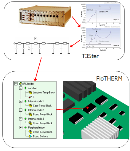 Simulation nowadays is the most common approach in deriving these so called CTMs (compact thermal models) but experimental methods continue to contribute. The TDIM approach detailed by JESD51-14 and introduced in the previous blog can identify the thermal resistance from the package junction to the heatsunk face without resorting to often erroneous thermocouple approaches. The unique structure function approach that the T3Ster measurement employs then provides a ladder of thermal resistances and capacitances from the junction up to the case. This can be used to create what is best to think of as an enhanced 2-resistor model, where Theta_jc is not a single value but a ladder of RC pairs. This experimentally derived resolution of the internal heat flow path within the package results in a CTM that is capable of Tj and Tc prediction and appropriate for transient or steady state simulation (transient in that thermal capacitances are present, something that’s missing from other standardised CTM approaches such as 2R and DELPHI).
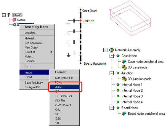 Both the JESD51-14 standard AND the subsequent creation of an enhanced 2R CTM is fully automated in T3Ster, including a direct interface to FloTHERM.
From experiment to simulation in a few steps, a great example of how the two approaches can work together to help alleviate the pains of the thermal design engineer.
5th April 2013 Ross-on-Wye