Bottlenecks and Interface Materials; Part 1 – Great Thermal Bedfellows
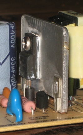
Probably due to the beer fridge, I now seem to be becoming the repository of broken electronic products with an expectation that the cause of their demise can be identified, retrospectively, using thermal simulation. This week my good colleague John Parry dumped a rather poorly DVD player on my desk with a ‘go on then’ look. There’s nothing quite like the sight of a scorched PCB to excite those of us working in the electronics cooling line of business here in the mechanical analysis division and that’s just what John and I found when inspecting the power supply board of this particular defunct DVD player.

I’m sure a wide variety of things have been photocopied, especially during company Christmas parties, but maybe never a PCB. It turned out to be the best way to capture the underside of the power board, both to capture the said scorching, also to get a map of the copper distribution that I’d need later when building the thermal model.
From a thermal perspective the TO220 amplifier was evidently the most critical component, the scorching was on the underside of the board directly beneath it. It was screwed to a vertical aluminium heat spreader with thermal paste used to achieve a good contact between the package case face and the spreader. Back in the day it took me a while to get my head round the idea that thermal contact between two objects can be enhanced by adding something else between them. The point being that you can never squeeze all the air out from between two solid contacting faces. Unlike moving air that is a great transporter (convector) of heat, stagnant air isn’t. Coming in at a tiny 0.026 W/mK (thermal conductivity) air is actually a great thermal insulator. Even the smallest amount of trapped air will cause a large thermal bottleneck. Getting goosebumps on your skin when cold is a Darwinistic throwback to that fact.
So, adding a paste/gel/putty/tape between the two objects will add some additional solid resistance but totally remove that pesky air resulting in an overall reduction in contact thermal resistance. That’s the theory anyway, unless you invest in a particularly cheap thermal interface material that can dry out, crack and lose its surface adhesion advantage. Why is it that cheap electronics always break? Go figure.
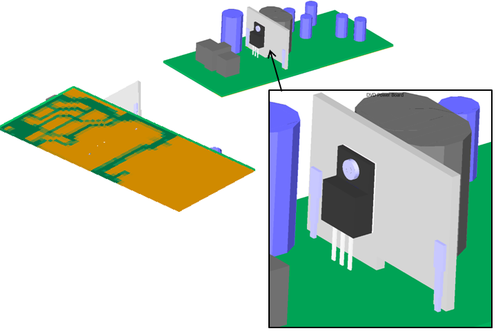
Building the FloTHERM model of the board was straight forward. The FloEDA application window allows for the import of populated PCB data to be imported directly from Expedition, Boardstation etc. Alternatively it can be used to quickly sketch out 3D PCB representations, including the layer stackup with the neat ability to import an image that represents the distribution of copper on each layer. For this board I imported the photocopier scanned image of the bottom layer then used FloEDA’s unique image processing capabilities to convert that into a thermal conductivity map of the distribution of FR4/Cu on the bottom layer.
The To220 detailed model was created using FloTHERM PACK. This involved a parametric definition of its construction and then pressing the ‘download detailed model’ button! The screw connecting it through the spreader plate and the spreader plate itself was manually defined in FloTHERM. The thermal interface itself was modelled as a 300 micron thick block with appropriate thermal conductivity.
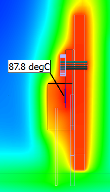 With an assumed dissipation of 2.0W the predicted junction temperature comes out at a respectable 88 degC. This model remember represents the ‘working’ design where everything behaves as it was designed to do.
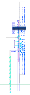 Examination of the heat flux vectors give further insight as to where the heat is flowing so as to produce the resulting temperature field. From the die, 85% of the heat passes through the thermal interface and on into the heat spreader. The other 15% passes down the leads, through the board to be spread throughout the bottom plane of the PCB where it is convected and radiated away to the rest of the DVD chassis.
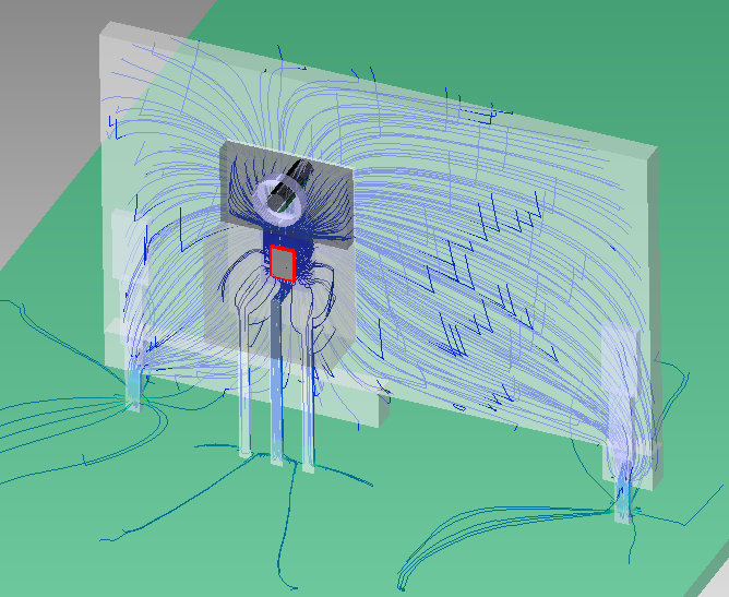
Taking 2D slices through a 3D model often doesn’t take into account the more complex heat flow paths the heat weaves through on its way from its source (die) to the ambient. Looking at lines of heat flux in a semi-transparent view of the geometry highlights an interesting heat flow feature…
If the aluminium spreader was big enough so as to do its job properly all the heat would pass through it and from its vertical faces on into the surrounding air. As can be seen from the heat flux lines, a certain percentage actually passes through its pins back down into the PCB. Further examination of the predicted heat flux values indicates that, out of the 1.7W that passes into the spreader, 0.46W (27%) necks down through the pins. A thermal resistance in itself.
Never liking to see a bad thermal design, it’s at this stage I tend to get all indignant and demand to know why FloTHERM wasn’t applied in the design of this product. And this is the intended design, we haven’t even got onto the thermal interface failure yet!! Ach, enough of the moaning already. In Part 2 we’ll get on to what happens when the thermal interface fails, using the display of the BN (bottleneck) number to help understand why and where the thermal design is deficient, allowing us to propose and simulate some targeted remedial thermal design modifications.
18th January 2012, Nottingham.