“All models are wrong, but some are useful” Part III
The next two parts in this series focus on the thermal model representations of electronic objects. The first being packages, or should that be components, or chips? From a mechanical analysis perspective they’re the things that are plonked onto a PCB that get hot. These things do clever electrical stuff, or should that be electronic stuff? If you haven’t already guessed I’m a mechanical engineer with a penchant for fluid and thermal effects, apologies for my somewhat uneducated use of electronical terminology 😉
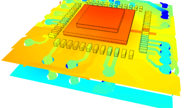
Either way, from the heat’s perspective the package is just the first stage in a series of resistances it experiences as it makes it way to the ambient (conversely it’s the last barrier the cold has to go through before it can quench the heat source). Under such conditions the heat flux is very high (this is the area into which the heat has to squeeze out (W/m^2)) and so any resistance the heat experiences will have a disproportionate effect on the source (junction) temperature. So, getting these thermal resistance right is key. When modelling a package there are two ways in which you can represent these resistances.
‘Detailed’ models
Such models contain explicit 3D representations of the internal construction of a package. A 3D object representing the die, with the correct material properties, with the power being set to dissipate on its surface. All the other important internal objects such as die attach, bond wires or leadframe, encapsulant etc. with their material properties. Very few assumptions about the thermal resistances are therefore made and thus the resulting accuracy is as good as you can achieve.

OK, so why are such package models rarely used? Not through want of trying that’s for sure. It comes down to the fact that component suppliers are unwilling to divulge what is seen as proprietary information regarding their package. What, like small minor design issues? No, whopping big ones like die size.
We provide a tool called FloTHERM.PACK (formerly Flopack) that has the ability to create thermal models of packages which are parametrically specified. The following is part of the design sheet for a TBGA:

Once parametrically specified a detailed model can be downloaded and used in FloTHERM or FloTHERM.PCB to conduct the actual thermal simulation. If things like die size are not known then sensible defaults are assumed based on the experience we have of the more common package constructions.
Some assumptions, or rather simplifications, are made for the detailed package model. Grid count can be minimized by representing all solder balls as a single lump of homogeneous material with a thermal conductivity representative of the fact that there is both air and solder in that volume of space (a common trick used often for lots of electronics thermal models).
Thermal Resistor Network
A thermal resistor network (sometimes referred to as a CTM (compact thermal model)) is the alternative method of package representation.
“As if CFD based electronics thermal simulation wasn’t involved enough. Why do you guys go and complicate things with lots of options and methods? Jeesh.”
The main advantage of a CTM is that such a description does not give away any proprietary information. It is ‘compact’ in that it’s a very simple representation but still ‘behaves’ (thermally) like the real thing. It is a bit abstract though in terms of getting your head round the concept…..
The inside of the package is represented as a collection of thermal resistances (degC/W) that link abstract points (nodes) up together. The topology of the network of resistances (how many nodes there are and how they are connected) is intended to represent the dominant heat flow paths the heat follows as it leaves the package. There will be internal nodes, e.g. one that represents the junction and peripheral nodes, e.g. one that represents the top of the package, one that represents the bottom etc. With the power dissipation value assigned to the junction node a clever program like FloTHERM or FloTHERM.PCB can solve this network to find out how much of the heat flows through the resistances and what the temperature values are at the nodes. All without requiring die size or any other explicit physical property of the package. Suppliers are happy, thermal engineers are happy. Everyone hug.
“Hey, hold on, everyone knows you don’t get something for nothing, what’s the catch with these CTM thingamajigs?”
Not surprisingly it’s accuracy. The CTM should behave the same as the detailed model regardless of what environment they are placed in. In reality if a great big heatsink is placed onto a package the heat removal paths will be different compared to when that same package is put on a board that is wedgelocked into a sealed enclosure where the heat is designed to be sucked down out through the board. It can well be that the resistor topology does not account for the (surprisingly) wide variations in heat removal paths. It may not be Boundary Condition Independent (BCI). A good CTM will be BCI. I won’t go into detail here about various ways in which a CTM can be derived. JEDEC have just issued some relevant guidelines for both DELPHI and 2-resistor CTM types if you want to read more.
 Block models and no model at all models
Both detailed and CTM models are capable of predicting junction and case temperatures thus providing the ability to judge thermal compliance. But what, if like the most of the real world, you can’t find any such models? The best you’ll be able to do is to model your package as a single block with a single thermal conductivity and assume the power is dissipated throughout that volume.
“Wow, sounds much easier. All I need is the footprint size, height and thermal conductivity…. Hey hold on, you nearly had me there again, so what’s the catch!?”
Well, knowing what thermal conductivity value to use that best represents the package as a whole aint easy. Somewhere between 0.5 and 10 W/mK. Buy FloTHERM or FloTHERM.PCB, we’ve supplied a whole bunch of values based on package style. Even then due to non-BCI behaviour accuracy will not be perfect (but then again, that’s the whole point of this series…).
The final component modelling ‘level’ is ‘no model at all’. For small passive surface mounts capacitors, resistors and the like they are so thermally passive that they will not effect the heat around them, they will simply assume the temperature that is coming from other more thermally dominant packages near by. Often you won’t care about such passives but if you do then just ignore them for the simulation but note the board temperature where they sit in reality, that will be = case = junction temperature.
Accuracy
“For a series that’s meant to be about accuracy you’ve just made me read 1100 words and I’m still none the wiser.”
Sorry, I do have a tendency to ramble but the following summary would not have much sense without the package modelling level background. All % errors themselves should have error bars associated with them. The following is a VERY ROUGH guideline. The errors are specific to just the component model and have been learnt through experience as opposed to formal study. Based on dTj rise over ambient, compared to ‘reality’:
- Detailed ~5%
- DELPHI ~10%
- 2-R ~ 20%
- Block – ~20% on case temp rise, unable to provide junction temp
These average errors should set expectations only. There are times when a 2-R model can be very accurate (for certain package styles when placed in certain environments).
Having the accuracy of a detailed model with the ease of definition, distribution and hiding of proprietary data of a CTM would be a great combination. Yep, sure would.
5th June, Ross-on-Wye