Simcenter STAR-CCM+ 2019.1: Plasma simulations at the edge of Moore’s Law
In 1965 Gordon Moore, co-founder of Intel, noted that the number of transistors in an integrated circuit (IC) doubles every year, and predicted this trend would hold for at least a decade. Later the periodicity has been revised, most commonly defined as 18 months, and has been consistently used for long-term planning and target setting for R&D in semiconductor industry. However lately there have been lots of discussions about the probable death of Moore’s law, since silicon-based semiconductor size is now approaching physical limits. Learning from history, the clock frequency stalled already ~13 years ago; check out the graph in this blog – although the number of transistors is still increasing the clock frequency stagnated around 4 GHz in 2006. This is due to hitting the “power wall” – the limit where leakage currents and heat production become significant enough to get faulty operation and overheating. Likewise, the transistor size cannot continue to shrink forever due to the finite size of the atom itself. The latest circuit printing technique available today allows for 7 nm structures on the chip. 7 nm – that’s ~70 atoms! Below this size, migration of single atoms may damage the nanostructures of the IC, and quantum effects start to interfere. Thus it is impossible to go much further with similar technology, and the consistent shrinking in transistor size from 1960’s to today, from mm to ~7 nm scale, is about to end. This doesn’t mean technology advancements are over, technologies such as 3D patterning, improved packaging, using materials with higher conductivity, smarter layout and coding, application-specific integrated circuits and far out potentially quantum computing still advances our computational efficiency. But, the era of ever-decreasing transistor size is over. ~7 nm may be the end.
What does this have to do with plasma, the fourth state of matter where electrons and ions roam free? Well, the technology that lets us get to 7 nm is Extreme UltraViolet Litography (EUVL), where 7 nm patterns are copied from a template to the wafer by ultraviolet light of 13.5 nm wavelength. The ultraviolet light is produced by photon emissions from a tin plasma. The EUV light is collected by a mirror and guided through the scanner to replicate the template pattern on the wafer. The mirror itself is exposed to the plasma, and is easily damaged by high energy ion impacts. Hence reduction of impact rate is highly desirable and any design changes which lowers the impact will extend the life time of the very expensive EUVL equipment. Simulations can aid design through analysis of plasma density, energy and extent. Even in the rest of the semiconductor manufacturing product line, which may consist of hundreds of fabrication steps, plasmas play a vital role; Lieberman & Lichtenberg noted in 2005 that one-third of the fabrication steps are typically plasma-based(!). Plasmas are used to etch wafers through plasma etching and to deposit materials on the wafer through sputtering physical vapor deposition (PVD) or plasma-enhanced chemical vapor deposition (PECVD).
To support technology development at the edge of validity of Moore’s law, Simcenter STAR-CCM+ adds plasma chemistry simulation capabilities in the upcoming 2019.1 release. This allows you to study electron number density, ion concentration and electron temperature in low temperature plasmas, such as used in EUVL, sputtering PVD and PECVD processes.
To be specific, now you can read in any plasma chemistry in standard CHEMKIN™ format in Simcenter STAR-CCM+, and solve the chemistry with the stiff chemistry solver CVODE, which is proven for its robustness and speed for combustion simulations.
For an example see an inductively coupled argon plasma etcher below. The coil in the top of the picture is inducing an electromagnetic field through an alternating current of 13.56 MHz, strong enough to rip electrons off neutral argon atoms. The electrons are accelerated by the electromagnetic field, giving them high enough energy to excite or rip off further electrons of other argon atoms, creating a plasma of excited argon atoms, argon ions, neutral argon atoms, and electrons. The purpose of this plasma is to etch the wafer surface through bombardment of argon ions.
The electron energy source from the electromagnetic field is shown on the left-hand side, and the corresponding cloud of free electrons on the right-hand side. The electron density peak is slightly further away from the Quartz crystal than the peak of the Electron energy source field since neutralization of electrons by the surface reduces the number of electrons close to the crystal.

The corresponding cloud of argon ions, which are used to etch the surface, is shown in the picture below. The argon ion cloud is very similar in shape to the electron number density since the electrons induce the ions.

The argon chemistry used in this simulation includes three reactions; argon excitation, ionization and stepwise ionization. The momentum transfer reactions are included in the model implicitly.

This is a somewhat simplified scheme. Extended schemes or schemes for other species can be obtained from Quantemol, an expert company within the field of plasma chemistry, whom we rely on for help and guidance.
The etching profile at the wafer surface needs to be as uniform as possible. To achieve that four different designs are studied:
-
- Table positioned 4, 5 and 6 cm from the crystal surface
-
- Coil and crystal widened by 4 cm.
First, the effect of table position is investigated. See below for visualisation of the electron energy source term from the electromagnetic field and the corresponding electron number density.

Note the increased electron density for lower table placement. The ions and electrons are neutralised by the walls, and thus the more space between coil and table, the higher the plasma density. A higher number of free electrons increases the plasma conductivity, which is why the electron energy source term also increases by lower table placement.
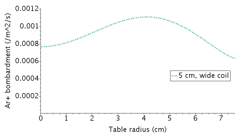
Next, let us investigate the effect on etching rate by plotting ion bombardment radially along the table surface, calculated through imposing a flux boundary condition at the surface. See the plot below.

Two things are notable here; The lower the table placement, the lower the ion bombardment, giving a lower etching rate. But the homogeneity is also decreased when moving the table further down, which is undesirable. This is due to the higher peak electron and ion concentration in the centre of the plasma.
Can we reduce the inhomogeneity by stretching the coil and thus stretching the plasma? Let’s try. In the picture below the coil and crystal is stretched by 4 cm.

The plasma is consequently more stretched out, and it appears the electron number density close to the table is more evenly spread than in the previous cases. Interrogating the ion bombardment at the table surface it is evident that, although there is still a significant peak, the bombardment is more evenly spread. The difference between main peak value and edge is 40%, compared to 70% for the baseline case.

The wider coil placement is thus a potentially better design for this etcher, and further studies could be made by varying inlet rates, pressure, number of coils etc.
I hope this serves as a demonstration of what can be learnt through plasma simulations.
With this new functionality in Simcenter STAR-CCM+ we hope to support the evolution of computational power at the edge of and beyond Moore’s law. Don’t hesitate to contact us for further information!
Learn more about plasma simulation using multi-physics software to model plasma processes in semiconductor fabrication in this webinar.