Ensure 3D IC Multiphysics Reliability for AI Systems at Scale

Every new generation of AI systems pushes SoC design teams closer to the end of Moore’s Law. The core question facing IC and package designers is whether existing 2D SoC workflows can still ensure system performance and reliability demanded by high-stakes AI systems?
The answer: moving to 3D ICs is no longer optional. Scaling AI computing now means scaling design complexity into the third dimension.
3D ICs stack multiple dies from different process nodes using thousands of interconnects, creating tightly coupled thermal, mechanical, and electrical interactions. At such a density, a single thermal, a single stress hotspot, or power integrity failure can propagate across dies, compromising system-level reliability.
This article examines multiphysics challenges in 3D IC designs and outlines three design imperatives to identify risks earlier and support PPA, reliability, and yield targets for next-gen AI systems.
Beyond 2.5D: Why 3D IC design breaks traditional workflows
It’s really getting harder to delineate where the chip ends and the package starts.
Kevin Rinebold, 3D IC Technology Manager
AI computational power (FLOP/s) is scaling at roughly 1.35X per year, nearly twice the rate of Moore’s Law. Multi-die integration, particularly 2.5D integration, has become the new engine for today’s AI systems. True 3D IC is rapidly maturing, driven by HBM stacking, vertical logic–memory co-design, and the need for higher bandwidth, lower latency, and better power efficiency.
While hyperscalers have moved first, the forces driving 3D IC designs are no longer confined to a handful of big players. According to Allied Market Research, the 3D IC market is projected to grow at 20% CAGR through 2030. This means design teams that cannot model and validate interactions across dies, packages, and boards will face increasing schedule and reliability risk. This shift introduces a new class of system-level challenges that traditional homogenous IC design workflows were not built to handle:
Multiphysics coupling
Thermal, mechanical, and electrical behaviors are tightly coupled across dies. Accurate power and thermal modeling hinges on capturing the full parasitic network for each die, their mutual couplings, and the entire assembly connectivity. For instance, comprehensive thermal analysis also must reveal how thermal cycling can exacerbate mechanical stress, with each phenomenon evolving on a different time scale.
Scalability of design methodologies
3D IC architectures and packaging technologies continue to evolve. The industry is moving beyond traditional CoWoS-S toward embedded silicon bridge technologies. Heterogeneous integration is expanding beyond HBM to include I/O dies and co-packaged optics. Meanwhile, new power delivery architectures and integration schemes are emerging. To adapt to this pace of change, an open and scalable workflow is critical to aligning new application requirements with manufacturability, yield, and cost.
Late-stage reliability issues
A growing share of 3D IC issues is discovered too late, during package integration or system bring-up, when fixes are costly or no longer possible. This is because siloed, “over-the-wall” workflows break down when electrical, thermal, mechanical, and manufacturing decisions interact continuously.
Listen to the Siemens 3D IC podcast episode as technical experts take a deep dive on these challenges.
Read on to explore three design imperatives for reliable 3D ICs in the AI era.
Strategy 1: Enable early system-level multiphysics modeling
You could stack chips together nicely and do a signoff analysis to check the power, heat, and stress. But the problem is, if you find a problem, you don’t have more time. You’re at the end of the design cycle.
John Ferguson, Sr. Director of Product Management
Most SoC teams discover the hardest lesson of 3D ICs the hard way: they’ve already locked in die-level physical decisions by the time reliability issues surface during integration. A 2D SoC design flow relies on high-level RTL descriptions, where many physical assumptions (such as power distribution and thermal limits) are fixed early. However, a chiplet that meets electrical and thermal specifications in isolation can fail to do so once stacked. This leads to conservative design rules, over-constrained layouts, or unforeseen system failures.
3D IC necessitates continuous multiphysics evaluation, starting as early as floorplanning and on through every design iteration. As designs mature and more accurate data becomes available, these models are refined, enabling incremental adjustments like reallocating chiplet placement, optimizing thermal vias, or adjusting dummy fills.
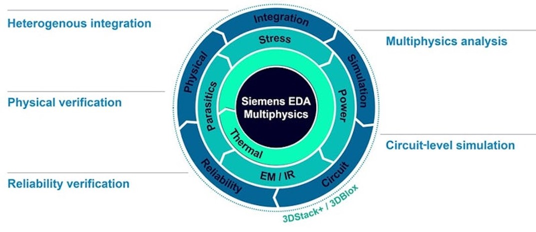
Siemens supports continuous multiphysics evaluation with a unified design environment that brings together Innovator3D IC Integrator and Calibre 3D IC solutions. This solution allows teams to model multiphysics effects early, inform thermal and stress-aware placement decisions, and consistently propagate those insights to board- and system-level analysis.
Strategy 2: Integrate thermal analysis from die to system levels
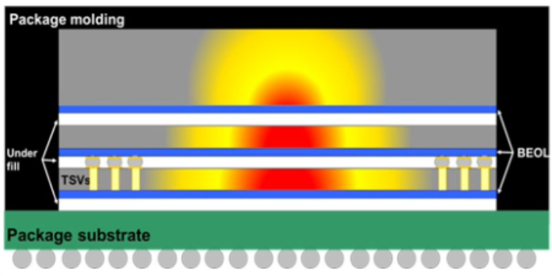
With multiple chiplets stacked in extreme proximity, 3D IC’s power densities can reach the order of magnitude of the surface of the sun.
Andras Vass-Varnai, Siemens 3D IC solution engineer
Maintaining 3D IC thermal reliability requires careful consideration of the following factors:
- The use of thinned dies (often less than 100 micrometers) limits lateral heat spreading.
- Through-silicon vias (TSVs) act as thermal conduits between layers, producing complex heat distribution patterns that must be accurately modeled.
- Micro-bump arrays influence local thermal resistance, while hybrid bonding interfaces introduce new complex thermal behaviors.
- Interposers extend thermal paths across the package, requiring closer coordination between design and analysis to fully understand and optimize heat dissipation.
- As layer counts increase, advanced packages often combine heterogeneous materials with vastly different physical properties. Anisotropic thermal conductivity, temperature-dependent material behavior, and nonlinear heat flow all become critical modeling considerations.
Rule-based thermal checks and template-based model building that work for 2D designs do not scale to these conditions. Package architects and design engineers need to be able to quickly assess thermal implications and identify potential temperature-limiting factors early in the architectural design stage.
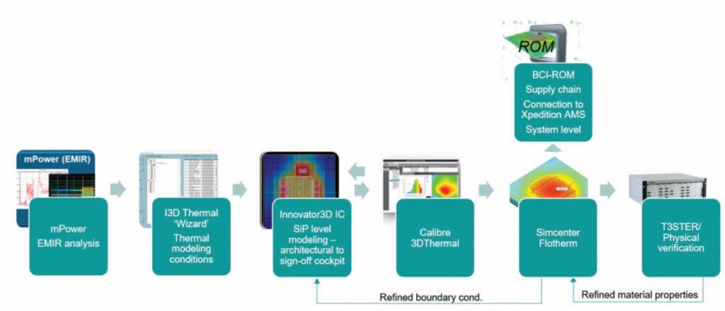
Siemens enables thermal-aware design with fully connected die-to-system workflows that integrate Innovator3D IC Integrator, Calibre 3DThermal, and Flotherm. While traditionally, chiplet, package designers, and thermal analysts work in different “silos” and communicate via specifications at best, our integrated approach allows engineers of various backgrounds to work on a shared database translated to their view of choice.
Listen to the full podcast episode for an in-depth discussion on emerging thermal management trends and system-level design practices in 3D ICs.
Strategy 3: Perform progressive verification to keep SI/PI in control
For 3D IC it’s a much flatter design process. The analysis you must do really has to be done early on and analyze the different pieces of the subsystems concurrently.
John Caka, Siemens Principal SI/PI Engineer
In 2D SoC design flows, signal integrity (SI) and power integrity (PI) analysis are typically performed in isolation and validated at the component level before full system integration.
Such a compartmentalized approach is inadequate for the inherent complexities of 3D ICs. The close physical proximity of stacked dies introduces new coupling mechanisms, shared return paths, and tightly coupled power delivery networks. SI and PI behaviors now interact across dies, interconnects, and packages, amplifying risk if issues are discovered late in the flow.
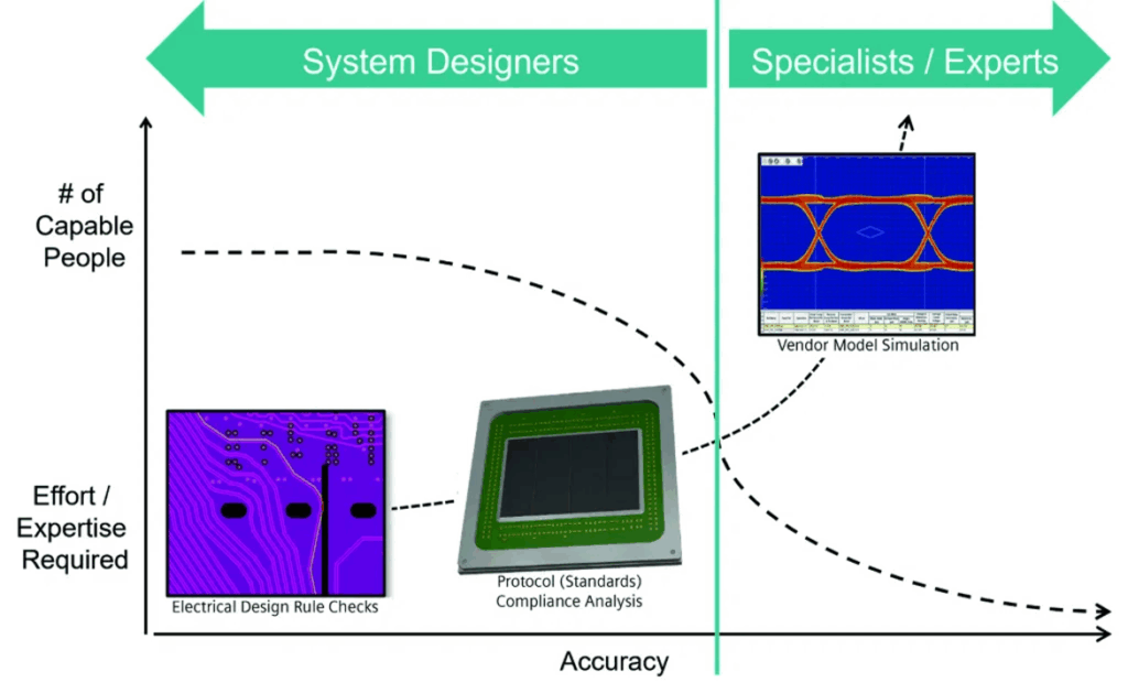
To streamline 3D IC SI and PI analysis, Siemens enables a progressive verification strategy, where design teams can start analysis as early as possible with minimal inputs, gradually adding detail as the design matures. As the design progresses through floorplanning and implementation, more in-depth analysis and optimization are performed, culminating in a final, detailed electrical analysis using vendor-specific IP and actual current values.
This iterative approach ensures that issues are identified and addressed continually, leading to a robust final design. Listen to the full episode as Siemens’ John Caka dives deeper into 3D IC electrical analysis challenges and solutions.
Improve 3D IC performance and reliability with Siemens
As 3D IC complexity continues to scale, reliability and system-level PPA increasingly depend on identifying multiphysics risks upstream, iterating against a unified model, and continually validating decisions across the entire stack.
Siemens empowers customers with a multiphysics-aware, die-to-system design approach that replaces stitched-together, point analyses with a coherent system view. By grounding architectural and implementation decisions upon a consistent understanding of thermal, mechanical, and electrical interactions, teams can achieve more predictable system performance as designs progress into next-generation AI systems.
Schedule a free customized demo to explore how to unlock system-level multiphysics insights for predictable, reliable 3D IC development.


