From silos to system: Sujit Sharan on the cultural and technical shift 3D IC demands

“The first call would be for all our EDA partners to shift from a tool-centric thinking to a system level thinking. We’ve talked about the fact that system level optimization is where we need to be — all of these tools over the years have gotten very efficient. The silicon tools, the package tools are all extremely efficient, but I think we need to look at the full stack holistically.”
Sujit Sharan, Intel fellow
What does it take for one of the world’s most complex engineering organisations to commit — fully — to 3D IC as a strategic direction? And what does that commitment reveal about the gaps the entire industry still needs to close?
What you’ll learn…
- (02:07) Sujit’s background: 30+ years in semiconductor processing and packaging, 300+ patents across X-ray lithography, CMP, and advanced thin film
- (02:07) The three vectors driving Intel’s 3D IC strategy: reticle size limits, AI/HPC memory bandwidth demands, and chiplet cost efficiency
- (04:33) EMIB for 2.5D lateral die-to-die interconnects, and Foveros / Foveros Direct for 3D vertical copper-to-copper hybrid bonding
- (06:48) Tackling design partitioning, thermal management, power delivery, and testability through STCO — System Technology Co-Optimization
- (09:45) The biggest ecosystem challenge: breaking down cultural silos between silicon, package, and board design teams
- (13:10) Why showing engineers real co-design data was the decisive factor in driving the mindset shift
- (14:33) The EDA gaps still needing breakthroughs: full-stack digital twin, integrated multi-physics simulation, and cloud-based collaboration
- (17:50) Killer app segments: AI and HPC, autonomous driving, communications bandwidth, and AI-driven EDA automation
- (20:16) What the 3D IC era demands of engineers: T-shaped skills, cross-domain awareness, and real-world trade-off thinking
- (24:57) Sujit’s call to action: shift from tool-centric to system-level thinking, build the digital twin, standardise data exchange
View the full episode transcript
Tova (00:00.000): Welcome back to the 3D IC podcast as we continue our journey through the intricate world of 3D integrated circuits and heterogeneous integration. I’m your host Tova Levy, and today we’re diving deep into the strategic shifts, technical hurdles, and future visions of this transformative technology. As we explore the ever evolving 3D IC ecosystem, we’re honored to bring you insights from the brilliant minds shaping its future.
Tova (00:00.000): Today’s conversation is a perfect example of why the 3D IC ecosystem matters so much. We’re talking with someone who’s been at the heart of one of the industry’s most significant strategic shifts, Intel’s move to 3D IC technology, and he’s going to share not just the technical innovations, but the collaborative challenges and ecosystem gaps that need to be addressed. Joining us is Sujit Sharan, an Intel Fellow in the Advanced Packaging Technology Manufacturing Organization at Intel Corporation.
Tova (00:00.000): Sujit has over 30 years of experience spanning semiconductor processing and packaging at companies like Hampshire Instruments, Micron Technology, and Intel, and has worked on everything from X-ray lithography and CMP to advanced thin film processing. Currently, Sujit is a key driver in developing and optimizing product performance and cost through innovative package architecture solutions, particularly focusing on advanced packaging architectures for die disaggregation, using both 2.5D and 3D interconnects. With over 300 issued patents and 30 published papers, Sujit is a true thought leader in this space. Sujit, thank you so much for joining us today.
Sujit Sharan (Intel) (02:15.000): Thank you, Tova. Thank you for the introduction and for the opportunity to talk to you. Really honored to be here.
Tova (02:30.000): So we’ll start from this strategic shift that I mentioned. Intel made a significant shift towards 3D IC technology. Can you tell us what specific internal drivers led Intel to cement 3D IC as a core strategic direction?
Sujit Sharan (Intel) (02:50.000): Absolutely. So there are couple of key vectors that drive the Intel to adopt 3D IC as a core strategic direction. And I think the industry is moving along with that. One of the key factors is that monolithic silicon dies are becoming fairly expensive. Silicon processing is very expensive. And to drive to a really large, reticle-sized die, both from a yield and manufacturing perspective, is fairly expensive.
Sujit Sharan (Intel) (03:50.000): Also, the die sizes are limited to a reticle size, which is roughly in the 23 by 33 millimeter range. So to build complexes which are larger than 23 by 33 millimeter would require stitching all these silicon dies together, which is where innovative packaging architectures like 2.5D and 3D start coming into picture, where we can create reticle complexes which are much larger than what can be achieved monolithically on a silicon die. For example, Intel’s roadmap shows us going to really, really large die complexes, 20X, 30X, 40X reticle complexes which would not be possible to print directly on a wafer.
Sujit Sharan (Intel) (04:50.000): The other factor which is very important for us is the AI and HPC segments depend on higher and higher memory integration with the entire reticle complex, which means having memory off-package slows it down. You don’t get the bandwidth that you need. Your latencies are a lot higher than what you would like. Getting memory as close, physically close to the reticle, to the silicon dies is critical for getting the performance that you need for AI and HPC segments. And in that regard, we have developed technologies. Intel of course has its own local interconnect technologies that drive integrating this high density, high bandwidth memory very, very close to the silicon so that we can achieve the bandwidth and latency that we require for this performance.
Sujit Sharan (Intel) (05:50.000): Additionally, breaking it into chiplets offers us the opportunity to drive to an improved or similar performance as a monolithic die but at a much lower cost point, which is also going to be very important because I think the amount of silicon that is now going into these systems is huge and to drive the cost down is a huge imperative. So on these three vectors, trying to drive the bandwidth, drive latency, go away from just a monolithic silicon but to go to very large reticle complexes, drives Intel to essentially go to 3D IC and 2.5D stitching solutions.
Tova (06:40.000): And at the same time, there are also key technology shifts that have enabled this. So can you tell us a bit about that?
Sujit Sharan (Intel) (06:55.000): Sure, and so the key technology enablers that we are working on is embedded base technology. So Intel was one of the first companies to invent the use of silicon-based interconnects to connect different silicon dies in the package. This was essentially driven from the fact that the organic packages, including newer RDL rules, do not offer the type of interconnect density that you can achieve from a silicon-based technology to drive the bandwidth and latency. So Intel has developed what we call the embedded bridge technology, or EMIB technology, which allows for a local silicon die to be embedded in the package and be used for local die-to-die and die-to-HBM interconnects. This is obviously a lateral connection, so you have a 2.5D stack where your connections between the dies is laterally done.
Sujit Sharan (Intel) (08:00.000): Intel also has developed Foveros technology, both solder-based and now in the newer configuration for a copper-to-copper hybrid-bonded base, where you do a far more vertical stacking, where you have dies which are stacked vertically and connect through vertical interconnects instead of going laterally between the two dies. We do believe that there is a space for both 3D and 2.5D interconnects where you would stack your XPU dies vertically and then go laterally to maybe a memory configuration or in the other scenario you also connect various stack dies through a local interconnect in the package laterally. And these are technologies that Intel has obviously been in the forefront of developing and these are opportunities that I see is what is going to help us drive the industry forward.
Sujit Sharan (Intel) (09:00.000): The additional benefit of course is that companies can use and Intel has been doing that. You have seen products from Intel where we mix and match chiplets from different foundry nodes as well as from different foundry vendors so that you can have your lower performance silicon pieces be on a N minus one or even on an N minus two node while your high performance chips are all on the N nodes, which would again be a vector that drives cost and efficiency.
Tova (09:45.000): That’s a great overview of the why behind the shift. 3D IC brings with it a whole new set of technical challenges, particularly in areas like design partitioning, thermal management, power delivery, and testability across multiple stacked dies. So how is Intel addressing these complexities?
Sujit Sharan (Intel) (10:15.000): So essentially we have been working with EDA tool vendors to develop integrated design analysis methodologies across the full stack. The key element that becomes critical is we need to be cognizant of the fact that co-design is now becoming very, very critical when you are trying to integrate a bunch of chiplets into a package. By co-design I mean an optimization across the entire system, what we would call STCO, System Technology Co-optimization approach, where we look at the silicon, package and the board as a whole and not be designing each piece individually and then stitching them together. That would obviously create inefficiencies in the whole design process.
Sujit Sharan (Intel) (11:20.000): And I think the big challenge right now is to work with the EDA tool vendors to develop a system that would allow us to look at the entire design process, the silicon design, the package and the board design as one holistic piece. In addition to that, we need to make sure that all of the analysis across the thermo-mechanical, the thermal, the electrical performance, are all tied together because we as design architects have to make trade-off choices between how do I optimize such that I hit my yield numbers, my manufacturing yield numbers, which are driven quite a lot by thermo-mechanical considerations. We meet our reliability goals, which are again driven by a lot of the thermo-mechanical and thermal capabilities. We manage our power and signaling to hit the performance goal, but also to meet the thermal goals.
Sujit Sharan (Intel) (12:25.000): I think the era of when we try to optimize each of these vectors individually is long gone. Once we start integrating so many disparate pieces of silicon into one package, we need to make sure that we consider doing everything together and look at the integrated approach and make sure that we take into consideration all of the vectors that go into providing a cost effective, performance-optimized package. That cannot be done by designing in silos.
Sujit Sharan (Intel) (13:10.000): The current approach is still that for us, we use and we have developed a lot of tools internally and working with EDA tool vendors is Intel specific, but we need to standardize these. The call would be is that we would like to have the EDA tools be able to allow me to run a lot of these scenarios and we’ll talk about it hopefully at some point in time is how would we standardize everything so that we can easily integrate the chiplets into a package and then take it onto a board and make sure that we get the full system level performance benefits.
Tova (14:05.000): So actually that’s something that Siemens is definitely advocating for a lot. So yeah, it requires quite a major shift there, shifting to the system technology co-optimization. So speaking of holistic solutions, pushing a new technology like 3D IC requires a robust ecosystem from EDA tools, as we mentioned, to materials, testing, and the entire supply chain. What have been the biggest challenges in building out this ecosystem from Intel’s point of view?
Sujit Sharan (Intel) (14:50.000): So for us, the big thing has been is that we need to drive, and we are driving towards it. I think we still have some ways to go, it’s a mind shift change. We have in the design community usually in the past have been working with silos where the silicon design team finishes the silicon design, passes it on to the package design team who then design the package and then pass it on to the board design team. And there was not much collaboration across these boundaries. Breaking down these boundaries between these communities is a major cultural challenge. It is not just from a collaborative perspective, but also for people in each of these domains to develop expertise or at least some knowledge across the different domains and to make sure that we take into consideration all of the implications of doing the silicon design and how it would affect the package and for the package designers to collaborate with both the silicon and board designers to make sure that what we do on the package is the right thing to do from a system level. And that I think is a big driver that we need to in the industry drive towards.
Sujit Sharan (Intel) (16:10.000): EDA tools are also siloed right now, I mean you have people use silicon tools which would be from different companies, package design tools from different companies and board design environments which could be completely different. We need to have also the EDA tools be standardized across these, at least from the perspective of having the ability to do a seamless data exchange across all of the design environments. Today the design tools do not very easily talk to each other. We would get silicon design tool output something and we need to probably massage it before I can read it into my package design tool and then similarly from the package to the board design tool. We need to have some level of standardization which is where we see something like Siemens’ Innovator 3D IC and other tools like that being an example that allows us to look at the whole design view holistically and not have to look at the pieces of design and write scripts to kind of integrate everything together.
Sujit Sharan (Intel) (17:30.000): I think the onus is on the industry and on the tool vendors to be able to seamlessly allow different formats to be adopted into a 3D viewer type approach. The analysis tools are also fragmented. We have analysis tools, again, available from different EDA vendors from different ecosystems, but the ability to analyze and be able to integrate these tools into the design environment is of great importance because time to market is a huge deal. Design times are getting shorter and shorter. The ability to be able to go ahead and do the analysis and design in a consolidated environment is going to be of great value. And that’s where I think the EDA tool vendors have a lot of challenges to both collaborate across and to have hopefully an industry standard play box, a sandbox where we can do all of the design and analysis across all the thermo-mechanical, thermal-mechanical, and electrical vectors.
Tova (18:50.000): Okay. So we’ll get to the role of the EDA vendors in a bit, but I want to focus a little bit on the human side of this. So you mentioned that package designers need to understand more about the silicon designer’s domain and vice versa. What were the points of resistance that you met in this process when you were trying to create this ecosystem internally and how did you overcome it?
Sujit Sharan (Intel) (19:25.000): I think the biggest thing is more about having the right expectations and for people to see the value of the approach. And I think that is coming from the front view now that we have. Once the engineers see the value of being able to do the co-design and they actually see real life metrics which says that, if I did this on the silicon, this is the advantage that I get on the package. We feed that to the silicon guys, or if the silicon guys tell us, hey, this is how I’d like to do the silicon because I can do certain things on the silicon, and can the package afford it, we show them the impact. Data, showing the data to the engineers was the biggest motivator. I think once people see the fact that when you design and do a co-design across all of these vectors and you get the performance improvement, you get the cost improvement, you get the other improvements in time to market and so on and so forth. The engineers buy into this very readily. I think we are a very data-driven company and to show the data from this approach is essential to driving the mentality change.
Tova (20:40.000): Interesting.
Tova (21:00.000): All right, so back to the role of the EDA vendors. How critical is their partnership in enabling Intel’s advanced packaging roadmap and what key EDA capabilities still need significant breakthroughs?
Sujit Sharan (Intel) (21:30.000): So we have been working a lot with all of the EDA vendors obviously and it is very essential because I think one of the other things is we don’t want to have non-industry standard solutions because that does make it more difficult and not so efficient. We have been working with EDA vendors to co-develop methodologies around how we do both design and analysis. For example, we in the 3D IC stack-up power delivery analysis is a big deal. We have worked with industry vendors, EDA vendors to develop methodologies which are now being developed into a tool so that we can do, for example, a power delivery analysis across the entire stack and not have to go ahead and do the analysis at silicon and package level and stitch them together manually. So that is critical.
Sujit Sharan (Intel) (22:45.000): But going forward, I think for me, the ideal state would be as a full digital twin across the entire silicon package board stack. And by digital twin, I mean is that I can run electrical, thermal, mechanical simulations in my design tool or in a 3D stack tool. I should be able to run all of my analysis and be able to at least fairly readily be able to change my design and see the impact to all of these different domains. So for example, I change the routing on my package, I should be able to see, this is what it impacts on electrical performance. This is my impact to my thermal performance. I should be able to run more digital simulations across the stack instead of today we run a lot of empirical data collection where you actually have to run the empirical experiments to get some of this data. And that, I think, is obviously very expensive, very time consuming, and the ability to be able to run these in the digital space, be able to have models which are robust enough to simulate this entire stack is critical so that we can run these simulations and actually be able to narrow down my architecture choices significantly in the design space instead of having to run experiments and then be able to narrow it down.
Sujit Sharan (Intel) (24:20.000): And that, I think, is going to be important. Currently, I don’t believe there is a single tool which can stitch all of these elements into a fully integrated analysis. Again, we had talked about this earlier. Standardized, industry-wide EDA formats would be needed. Obviously, different companies, different groups, use different design tools in the different spaces. But to be able to stitch everything again together into one stack viewer is going to be critical. Cloud-based collaboration is going to be critical because now, obviously, everybody is a global engineering team. You have organizations working across the globe, and the ability to be able to work on design and analysis databases simultaneously across the entire globe is going to be critical. So I think cloud-based computing is going to be important. There’s going to be a lot of collaboration. These designs are now complex enough. There is no one single point of contact which can do everything. You’re collaborating across not just different expertise teams but also across different global locations and the ability to be able to look at everything into one place is going to be important.
Tova (25:50.000): Okay, so it’s clear that we need a robust and integrated EDA ecosystem. And looking ahead, which application or market segment do you believe will be the real killer apps that fully leverage the advantages of 3D ICs and heterogeneous integration?
Sujit Sharan (Intel) (26:15.000): Well, I think the starting point obviously which is driving a lot of this technology are the AI development at the high performance computing sectors. As you can see, I mean all of the AI companies are driving to these large form factor chips and package systems which can allow them to develop all of the AI models robustly enough. There’s a massive computational demand and that is driving the need to have and integrate a huge amount of silicon into a package. Memory integration drives a lot of the AI vector, so that again plays into the 3D IC space, and I think AI is one of the biggest engines driving this, which obviously is required for a lot of other work that we are doing. Autonomous driving is coming into play, requires a huge amount of computational power, both locally within the automobile as well as at the server level, and these are items that will drive that from a very, very much an engineering perspective.
Sujit Sharan (Intel) (27:45.000): AI driven, EDA design automation is going to be huge as to, I think the amount of integration that we have to do drives us to be able to delve into design scenarios far more rapidly than we have been doing today. We need to be able to iterate different architecture solutions and be able to get data from that using AI engines and using simulations to drive to proper solutions instead of waiting to run full experiments and then get data back and then be making those decisions. So I think these are things that will drive it. Obviously, communications is huge. I think the amount of bandwidth that it requires both locally as well as globally is going to be huge. How fast can you have data move around is going to be huge. Within the rack I think going from a standard board to board connection to going to top side connectors, bottom side connectors both powered by copper and then obviously at some point going to optical interconnects is going to be huge to drive local interconnect densities and local integrated bandwidths.
Tova (28:50.000): Right. I know that one of the things you mentioned, the design scenario exploration, that’s already something that’s been implemented in Siemens Innovator 3D IC solutions. So that’s an interesting one you mentioned. So moving on to a different angle of the 3D IC ecosystem, I want to talk about the people. In such a complex and multidisciplinary domain, what kind of people, talents, skill sets are most in demand?
Sujit Sharan (Intel) (29:35.000): Like I said, we have a lot of experts in the field, but I think we also need to develop engineering talent across the disciplines where people don’t just look at their own domain area, but are able to at least have a very good understanding of things that are slightly outside their domain, but affect their domain. For example, the electrical engineers who do the electrical performance analysis should have a fair understanding of thermal and mechanical aspects of it because we are not optimizing just for their domain. You need to be able to think more broadly. And so I think engineers need to be able to think outside the box and be able to essentially have at least a fair understanding of how changes that they make for optimizing their domain impacts other areas. This is critical because any decision that you make in one area, it ripples across the entire system and be able to understand and be able to mitigate those ripples is important.
Sujit Sharan (Intel) (30:50.000): Obviously, in a personal space, they need to have a very good collaborative mindset, willing to be able to learn and work across all of the different design aspects that we have talked about across silicon package and board teams, be able to be comfortable with being able to do trade-off analysis and compromise on things to make the system work. No one domain is going to drive the entire system. I mean, there’s no point having a very, very optimized electrical performance when you can’t manufacture it at cost. So being able to have the ability to see how cost, time to market, yield impacts your decision is very important. I think basically we have to have engineers who can think a little bit more broadly, be aware of the real world constraints, time to market, cost, manufacturing, as well as technical elegance of the solution. I think sometimes we look at technical elegance as the forefront of everything, but I think you have to look at broadly all of the real world scenarios and then of course being open to learning and driving because this area changes so rapidly. What you learned in school today is not necessarily going to be what is going to be implemented in the field maybe five years later. So openness to learning and driving solutions beyond your immediate area is also key. So in a nutshell, be able to collaborate, learn from other domains, be open to learning, and it’s critical for engineers to drive these solutions.
Tova (32:45.000): So how would you recommend, you know, for the engineers listening to us, how would you recommend, you know, for designers and engineers to prepare themselves for this sort of skill set that they’re going to need?
Sujit Sharan (Intel) (33:10.000): So I think first of all is obviously build a strong foundation in your own domain. I mean, if you are a mechanical engineer, obviously you build your strength in your mechanical engineering analysis. If you’re electrical, you work in and develop your skill set in your area first. So you have to build a deep expertise in your own domain, and that is still very valued. I mean, that is your starting point. That’s your foundation for your buildup. But then beyond that, then you start looking at taking and developing an interest as well as a key learning, take more courses in areas outside your specialty, learn if you’re an electrical engineer, learn some of the thermal and thermo-mechanical concepts. If you are a mechanical engineer, have an idea of electrical engineering implications, at least at a high level, so that you have an understanding and be able to discuss the trade-offs with your counterparts more efficiently.
Sujit Sharan (Intel) (34:25.000): Our learning and in Intel, we encourage that highly as collaborative and prosperous and working actively with senior engineers who have done this for a while and learn from their experience. That is going to be extremely important. We have talked about being open to learning and driving solutions across different disciplines. And overall, I think it’s just having an open mind and having the ability to learn and be eager to learn about other areas apart from your own. And you also have to keep learning in your own area because things change. You’re going to be getting new tools, you’re going to be getting new challenges, and having your deep expertise is important and I think in the past it used to be a lot more about the deep expertise. I think you need now both the depth and breadth of knowledge is required to drive good design solutions.
Tova (35:50.000): That’s so much more challenging. Yeah.
Sujit Sharan (Intel) (36:05.000): It is absolutely and I think that’s where I think a lot of the newer engineers and I think for me also talking to some of the younger engineers, I learned a lot from them. I mean they come with a different perspective and I think the ability to talk to people and learn from the different perspective is critical.
Tova (36:40.000): Alright, so on to our last question for today. So what would be your call to action for ecosystem partners? And what do you wish your partners understood better about what 3D IC requires?
Sujit Sharan (Intel) (37:10.000): So the first call would be for all our EDA partners to shift from a tool-centric thinking to a system-level thinking. We have talked about the fact that system-level optimization is where we need to be. Which is that, I mean all of these tools over the years have gotten very efficient. The silicon tools, the package tools are all extremely efficient, but I think we need to look at the full stack holistically. I think we have started doing that in the industry striving to developing a 3D stack tools, but I think a lot of it is still very much in its infancy. I think, for example, Siemens Innovator 3D IC is a step in the right direction, but it needs to expand further.
Sujit Sharan (Intel) (38:25.000): The ultimate goal, like I said, is to have the ability to be able to do a digital twin in your computer. I should be able to run things in my design or in my 3D stack tool, bring in my design database, bring in my analysis tools across all the segments, be able to run a full analysis on my 3D design, and then be able to tweak my design and see the impact to all of the different parameters that I’m looking towards by yield, by manufacturability, by thermo-mechanical constraints, thermal constraints, electrical constraints, and be able to get almost real-time feedback on that. I think the ability to do a digital twin is going to be critical, but I think, as you know, costs are spiraling. We cannot keep running a huge amount of silicon just to do a slew of experiments to validate all of the different aspects that we may be thinking of. It’s not that doing the actual builds are always going to be there, we’ll always be running these experiments, but the ability to narrow it down significantly in the digital space is going to be critical to manage both time to manufacturing, which again impacts you for cost and for performance.
Sujit Sharan (Intel) (39:55.000): Driving standardization is going to be critical. I mean, the ability to be able to seamlessly share data across different tool sets and different vendors’ tools and different domains is going to be critical. Right now, we do have to do a lot of manipulation to be able to read data in from different sources, be able to stitch them together. It’s going to be critical that we have some industry standards decided, worked on by the EDA tool vendors to make sure that there is an industry standard data sharing approach to be able to pull in data from different sources and be able to stitch them into one holistic whole. And then of course we have talked about the fact that we have people working on design across not just different domains but different geo locations to be able to have everything seamlessly and with minimal lag be able to run design scenarios in different geos so that if an engineer somewhere in Asia is doing a change to it, I can real time see it in my system here or in Europe or anywhere else and be able to react to it fairly seamlessly.
Sujit Sharan (Intel) (41:15.000): So I think overall, I think standardization is key. Building the 3D stack tools is going to be key. Integrating the design and analysis tools into one stack, when I say design tools, I mean the silicon package and board, everything designed into one stack. But that would be, I think, an ideal solution which we would love to see come to fruition pretty soon.
Tova (42:10.000): Yeah. All right. Data standardization has been mentioned several times on this season already. Yeah. All right. Sujit, this has been a really great conversation. Thank you for sharing your time and knowledge with us today.
Sujit Sharan (Intel) (42:40.000): Thank you very much, I really appreciate the time and opportunity actually, really appreciate the opportunity.
Tova (43:00.000): To our listeners, thank you for tuning in to the 3D IC podcast. Today’s conversation with Sujit really highlighted what this season is all about. Understanding that 3D ICs aren’t just a technical challenge, they’re an ecosystem challenge. We heard about the cultural shifts needed to break down silos, the critical partnerships with EDA vendors, and the collaborative mindset required to make this technology not just technically possible, but commercially successful. Join us next time as we continue exploring the innovations, challenges and brilliant minds shaping the future of the 3D IC ecosystem.
In this episode of the Siemens 3D IC Podcast, host Tova Levy speaks with Sujit Sharan, Intel Fellow in the Advanced Packaging Technology & Manufacturing Organization at Intel Corporation. With over 30 years in semiconductor processing and packaging and more than 300 issued patents, Sujit is one of the industry’s foremost voices on making 3D IC real at production scale.
Three forces drive Intel’s 3D IC strategy: reticle size limits on monolithic die; AI and HPC bandwidth demands requiring memory physically close to compute; and the cost efficiency of chiplet disaggregation. Intel’s response is EMIB (Embedded Multi-die Interconnect Bridge) for lateral 2.5D die-to-die and die-to-HBM connections, and Foveros / Foveros Direct for vertical 3D stacking via copper-to-copper hybrid bonding — complementary technologies, not competing ones.
Managing this complexity means abandoning the silo model. Sujit’s answer is STCO — System Technology Co-Optimization — treating silicon, package, and board as one integrated system. Cultural resistance was real; the solution was data, showing engineers the measurable gains co-design actually delivers.
The ultimate EDA goal is a full-stack digital twin spanning electrical, thermal, and thermomechanical analysis with near-real-time feedback. Siemens’ Innovator 3D IC is a step in that direction, but standardised data exchange and cloud-based collaboration remain critical gaps. Sujit’s call to action: EDA partners must shift from tool-centric to system-level thinking — and the whole industry needs to move together.
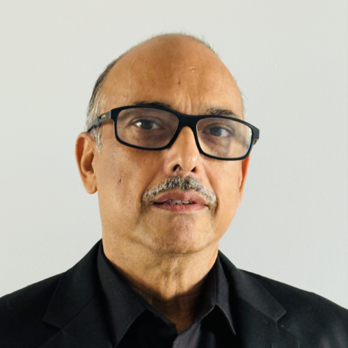
Sujit Sharan
Sujit Sharan received his bachelor’s degree in Materials Science from IIT Kanpur, India and a Ph.D. in Materials Science and Engineering from NCSU, Raleigh, NC. He has over 25 years of experience in semiconductor processing and packaging areas working for Hampshire Instruments, Micron Technology and Intel. He joined Intel Corporation in 2000 where he is currently an Intel Fellow in Advanced Packaging Technology Manufacturing Organization. Sujit has vast experience in the semiconductor industry having worked in multiple areas of the semiconductor industry, including x-tray lithography, CMP and advanced thin film processing. Before joining Intel, he worked for Micron Technology developing new interconnect technologies for DRAM and Flash memory. Currently, he is working on developing and driving optimized product performance and cost through innovative package architecture solutions. He has over 300 issued patents and over 30 published papers in academic and refereed journals, He has also given multiple invited talks at various conferences including IEEE interconnect conference and MRS.

Tova Levy
Tova Levy is a seasoned Content Producer and Manager at Siemens EDA, where she leverages her strong background in digital and content marketing strategy to plan and execute impactful content across various channels. Driven by a never-ending curiosity, Tova excels at distilling complex technical information into engaging, empathy-driven stories that resonate with B2B audiences. Her expertise lies in uncovering user pain points to create compelling narratives, consistently driving engagement and educating within the EDA technology space. Tova also produces the 3D IC podcast, transforming intricate engineering concepts into accessible, user-centric conversations.
3D IC
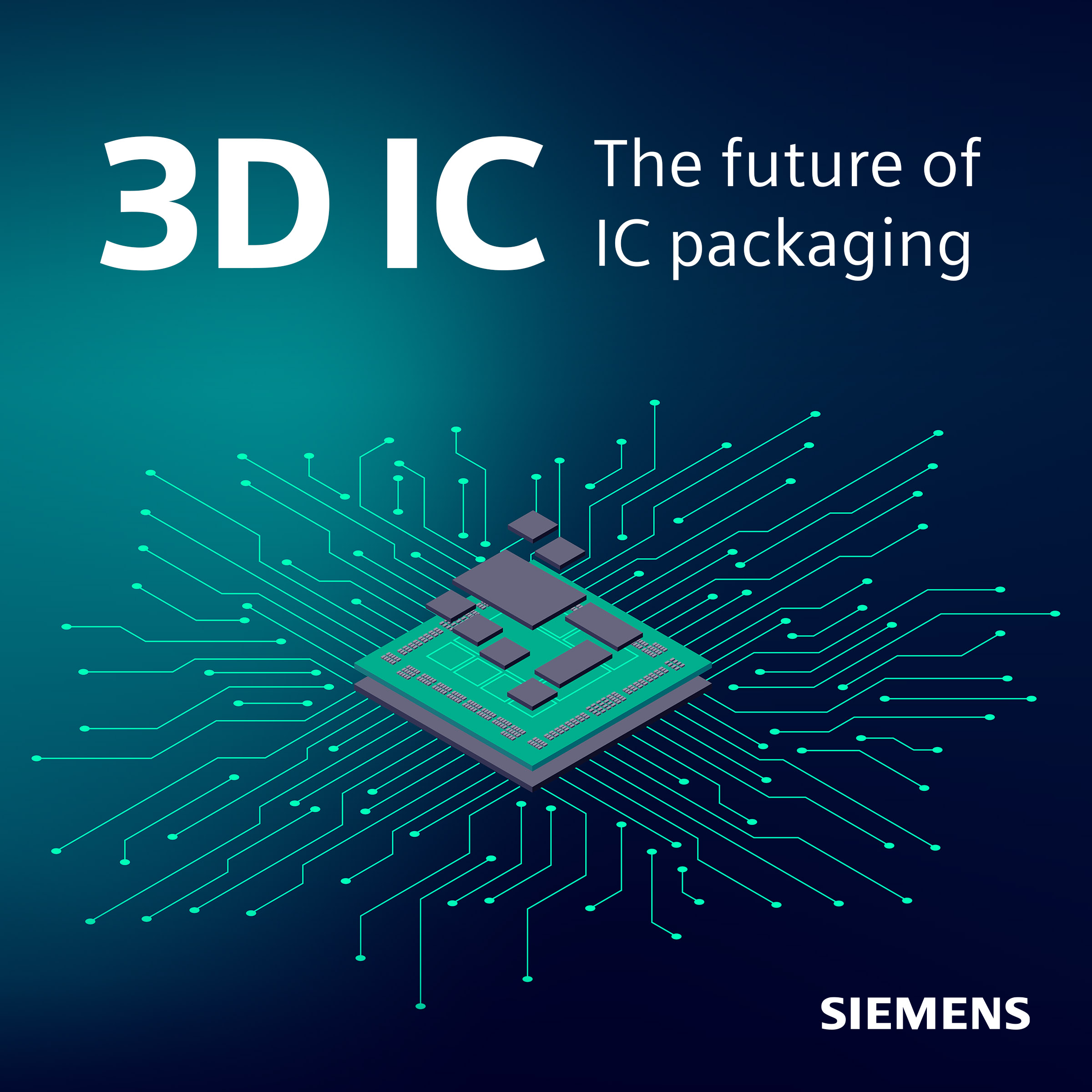
3D IC is the future of IC packaging. Learn with us how to prepare for it.
Listen on:


