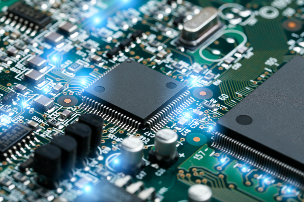
Component Placement: The Importance of Proper Placement for PCB Design
PCB design is a complex process that involves multiple factors, including the placement of components on the board. Proper component placement is critical to achieving an optimized design that meets manufacturing requirements. PCB designers may want to learn about the best practices for component placement, including keeping components away from each other to prevent interference and ensuring proper clearances for assembly and testing.
Why is Component Placement Important?
Component placement is an essential aspect of PCB design because it can impact the functionality, reliability, and manufacturability of the board. Improper placement of components can lead to various problems, including signal interference, thermal issues, and difficulties in assembly and testing. By placing components strategically on the board, designers can optimize the performance and reliability of the PCB.
Best Practices for Component Placement
To ensure proper component placement, PCB designers should follow a set of best practices. Here are some key factors to consider:
Keep Components Away from Each Other
One of the most critical considerations for component placement is ensuring that components are not placed too close to each other. When components are placed too close, they can interfere with each other, leading to signal integrity issues, noise, and other problems. To prevent interference, designers should keep sensitive components, such as oscillators, away from noisy components, such as high-speed digital circuits.
Ensure Proper Clearances
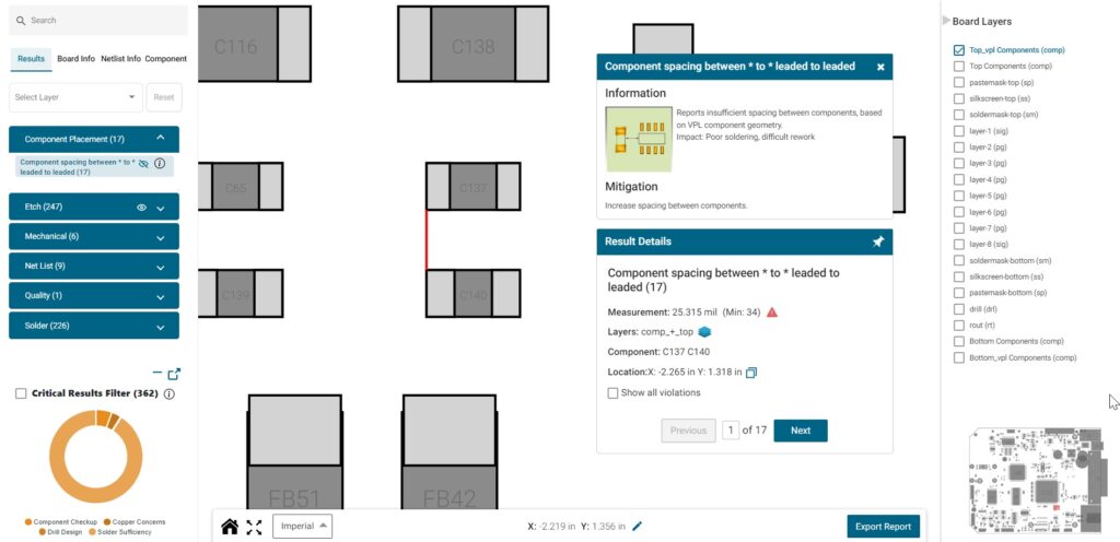
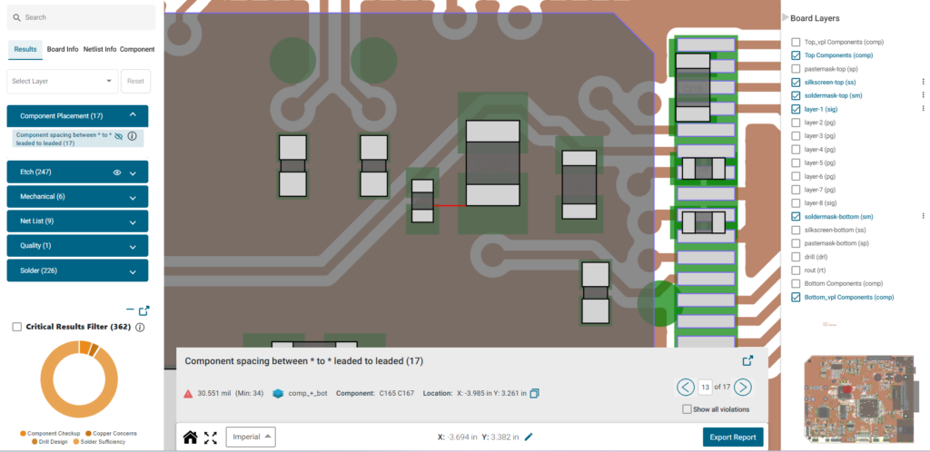
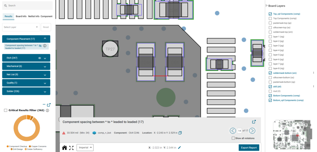
Another crucial factor to consider is ensuring proper clearances between components. Clearances are necessary to ensure that components do not touch each other during assembly, testing, and operation. Improper clearances can lead to shorts, opens, or other failures. Designers should follow the manufacturer’s recommended clearances for the specific components being used and ensure that they are sufficient for the assembly and testing process.
Consider Thermal Issues
Heat is a significant consideration in PCB design, and components generate heat during operation. Therefore, designers should consider thermal issues when placing components on the board. Components that generate a lot of heat should be placed in areas with good ventilation or with cooling mechanisms, such as heat sinks or fans. Designers should also ensure that components with different thermal requirements are not placed too close to each other.
Follow Design Rules
Most PCB design software provides design rules that ensure that the design meets manufacturing requirements. These rules include clearance, trace width, and other parameters that must be followed to ensure that the board can be manufactured and assembled correctly. Designers should follow these rules carefully to ensure that the board can be produced and tested successfully.
PCBflow Interactive Viewer
Conclusion
Proper component placement is critical to achieving an optimized PCB design that meets manufacturing requirements. Designers should follow best practices, including keeping components away from each other to prevent interference, ensuring proper clearances for assembly and testing, considering thermal issues, and following design rules. By following these guidelines, designers can create reliable, high-performance PCBs that meet the needs of their intended applications.