Silkscreen – is it really that simple?

A silkscreen contains human- and machine-readable marks on the surface of a PCB that indicates PCB components’ positions and polarity, test points, warning and standardization symbols, logos and other information about the board. The silkscreen is applied using non-conductive ink, whose standard color is white, but other colors are available as well. The silkscreen is applied to the bare board during the final fabrication stages, and is mainly used as a guide for board assembly, testing, and later – maintenance and repair.
What can go wrong with silkscreen?
During the data preparation for the PCB fabrication process, the CAM engineer treats silkscreen layers with the following goals in mind :
- The silkscreen should be sufficiently distant from solder mask clearances.
- The silkscreen should be readable.
The first aspect is of the utmost importance for the fabricator. Since silkscreen ink is not conductive, it can damage the quality of electrical contacts when it mistakenly protrudes into a solder mask clearance , possibly resulting in the scrapping of assembled boards if the flaw is not identified during electrical tests. So, in order to ensure the board’s quality, the standard procedure in most fabrication pre-production processes is to clip the silkscreen to keep a minimum required distance from solder mask clearances, as seen in Figure 1. The required distance between silkscreen elements and solder mask clearances depends on the silkscreen process and its accuracy – which might differ from manufacturer to manufacturer. Naturally, clipped silkscreens become less readable , and in extreme cases – not readable at all.
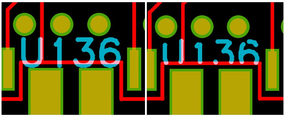
In the above example, the silkscreen (blue) is close to solder mask clearances (green) on the left. On the right, the silkscreen is clipped to keep it away from the solder mask. The red color denotes copper features.
But even if the silkscreen is kept safely distant from solder mask clearances, its readability may be affected by other factors, such as proximity to the board’s edge, proximity to tooling or mounting holes, or location under components. All these factors should be kept in mind when locating silkscreen elements on the board.
Last but not least: different silkscreen processes and machinery impose a variety of limitations on minimal line width and character dimensions. For example, a Liquid Photo Imaging (LPI) process is usually limited to a four mil line width. There are technologies that allow the printing of finer lines, but they are more expensive and might not be available where your board is being fabricated.
So what can be done?
In order to assure your silkscreen’s readability, make sure that it is located safely away from all other board elements that might impact its readability, especially solder mask clearances. At the same time, you should make sure your silkscreen elements are drawn using a line width that fits the manufacturing capability of your fabricator, as well as minimum height and width of individual characters.
PCBflow can help
PCBflow is Siemens’ online Design-for-Manufacturing tool. Developed for use by board designers mainly in start-ups and SMEs, PCBflow provides immediate feedback on design errors and violations, thereby reducing the number of board spins, cutting costs, and reducing time-to-market.
When using PCBflow, the required distances between the silkscreen and the different board elements are built in to a manufacturer’s DFM profile – as well as an array of silkscreen manufacturing capabilities and tolerances. With PCBflow, the board design undergoes DFM analysis against the manufacturer’s DFM Profile – and reports on silkscreen violations and many other types of potential errors.
PCBflow runs in a secured cloud environment, so you can rest assured that your IP is fully protected.
Sign up and try it out now at https://www.pcbflow.com/.