Modern day PCB design in the age of AWS cloud (Part 1 of 3: Unleashing new horizons)
In the world of printed circuit board (PCB) design and analysis, the strategic partnership between Siemens EDA and Amazon Web Services (AWS) marks a significant milestone. As businesses have increasingly embraced remote work environments, especially in response to the COVID-19 pandemic, the demand for robust, scalable, and collaborative tools has surged. The Siemens EDA partnership with AWS highlights how cloud PCB design infrastructure delivers new ingredients that will continually enhance the industry.
Main challenges in the industry
Traditionally, PCB design tools were downloaded and installed on localized computer hardware with teamwork best facilitated by the close physical proximity of team members. However, the landscape changed drastically with the onset of the pandemic, accelerating the need for distributed teams to operate effectively from various locations. This shift posed significant challenges:
- Collaboration: Teams scattered across different geographies needed tools that allowed seamless collaboration beyond the conventional on-premises methods.
- Accessibility: There was an urgent requirement for tools that could be accessed from anywhere, without the need for complex setups or high-end computer hardware.
- Adaptability: The tools needed to quickly adapt to the changing demands of projects and scalability to handle varying workloads efficiently.
Cloud PCB design functionality enabled by AWS
AWS has been instrumental in addressing these challenges by enabling Siemens EDA to enhance its PCB design and analysis tools with cloud capabilities. The key functionalities provided through AWS include:
- Hybrid cloud solutions: By integrating native cloud capabilities with existing desktop tools, Siemens EDA offers fully integrated hybrid solutions that combine the continuity and existing know-how of traditional desktop applications with the power and flexibility of the cloud. This approach also facilitates rapid feature enhancements and allows for greater computational power when needed, such as in running more compute-intensive applications like design for manufacturability (DFM) analysis.
- Enhanced collaboration: AWS’s infrastructure enables a range of collaboration tools that are integral to modern PCB design workflows. These tools help in real-time sharing and collaboration on designs, e.g., design reviews utilizing comprehensive 2D & 3D viewers with markup, ensuring that all product team members are on the same page, regardless of their physical location. Further, collaboration with external 3rd-party stakeholders has been completely transformed. No more lengthy email threads or the resulting discontinuity from differing means of information exchange. All stakeholders will be aligned to the single source of design/collaboration data.
- Scalability and availability: AWS’s global infrastructure ensures that the resources needed for demanding computational tasks and storage needs are always available and can scale based on the project’s requirements. This is particularly important for performance critical tasks such as handling large-scale simulations and real-time data analysis.
- Rapid deployment and continuous integration: The cloud environment fosters a culture of continuous integration and continuous deployment (CI/CD), enabling Siemens EDA to roll out updates and new features swiftly and reliably. This agility helps deliver better overall solutions to customers in the fast-evolving tech landscape.
The strategic partnership between Siemens EDA and AWS illustrates the transformative power of cloud PCB design. Through AWS’s robust cloud capabilities, we not only address the immediate challenges posed by distributed teams but also sets a new standard for innovation and efficiency in PCB design and analysis. As we look to the future, the deployment of cloud PCB design is expected to accelerate, further enhancing collaboration, scalability, and performance across the electronics industry.
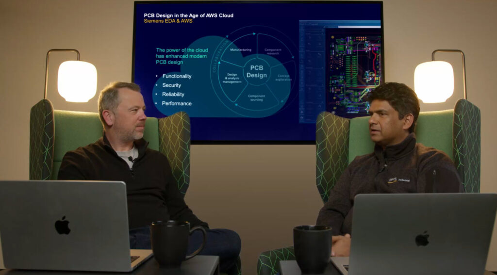
To learn more about how Siemens EDA is harnessing the power of AWS Cloud, tune in to this enlightening conversation between Adam Cabler (Siemens Chief Cloud Architect, Electronic Board Systems) and Azim Siddique (AWS Principal Solutions Architect).
Stay tuned for Part 2 of our series, “Securing the collaborative process,” that will drop soon to our three-part exploration of modern day PCB design in the age of AWS cloud.