ABCs of PCBs – K for Keepout
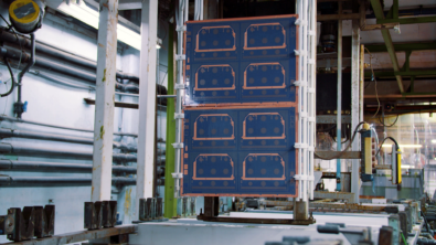
Welcome to ABCs of PCBs – a blog series to help new engineers learn about the world of Printed Circuit Boards. I’ll be covering topics from general engineering concepts to PCB design specific rules. As this is a ‘basics’ blog, I’ll keep the content software independent, but any visuals will be from the Mentor PADS Professional PCB suite.
If you missed the last post in this series: ABCs of PCBs – J for Jitter click here!
Have you heard of Keep Out? Apparently, it’s a popular game that’s making a comeback… but I’m focused on the PCB related definition. It’s fairly self-explanatory and may seem basic, but keepouts can make or break your first pass at creating a printed circuit board.
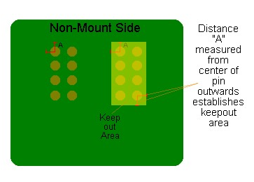
Keepouts prevent the placement of specific or all design items within a specified area. These design items can include electrical and mechanical devices – but also routes, surface mount pads, vias, etc. But why are these useful?
Often, a team of engineers gets involved in creating a finished PCB design. You may have an engineer who works on the schematic, another for analysis, and a different designer working on the layout. When you have different specialists working on the same project, there’s a chance an “obvious” design note like a restriction might get lost. For example, imagine you have a component that requires a heatsink, like a voltage regulator. You’re going to want to plan ahead, with the final assembly in mind, by providing room to add that heatsink without interfering with other components or elements on the board.
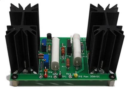
This is fairly obvious from the example above, but if you don’t assign a keepout area around the voltage regulators, there is a high chance of inadvertently placing a component within the area required that interferes with the heatsink. You might not run into this typical procedure in your senior design class – where you might be the only engineer working through the design process – but imagine how easy and costly it could be to miss this step. It’s an easy thing to overlook, but fortunately, a simple issue to avoid with keepout assignments.
Keepouts don’t necessarily need to be physical areas on the board that are avoided they can also be requirements set during the layout process, like assigning height restrictions. If you have a 3D model of what the enclosure looks like, you’ll have restrictions to make sure your board and its components are encapsulating. Consider the heatsinks in our voltage regulator example above. Adding a height restriction keepout in the z-axis in the layout can ensure the PCB will fit into its enclosure or if a lower profile heatsink should be used.
Whether you designed both the board and enclosure or two teams were involved, it’s important to track and share keepout information. Communication between your PCB design tool and the mechanical model is key when putting together an end product.
It’s always better to have restrictions like keepout areas set on your design instead of trying to remember – no matter how simple it may seem. You never want to realize your design failed because of a simple misstep that could have been avoided with 30 seconds of planning.
Thanks for reading and see you next time for more on the ABCs of PCBs.
-Shivani Joshi