ABCs of PCBs – C for Constraints
Welcome to ABCs of PCBs – a blog series to help new engineers learn about the world of Printed Circuit Boards. I’ll be covering topics from general engineering concepts to PCB design specific rules. As this is a ‘basics’ blog, I’ll keep the content software independent, but any visuals will be from the Mentor Graphics PADS Professional PCB suite.
If you missed the last post in this series: ABCs of PCBs – B for Board Layout click here!
We can find guided limitations or constraints – either provided for us or created by us – everywhere in our lives. They’re usually there to keep things orderly and functional. Time constraints show up in the example of getting your homework done on time for a shot at a good grade. Financial constraints create a bound for how much money to spend or budget for the future. No shirt, no shoes, no service is commonly used in establishments where that attire (or lack thereof) is acceptable outside, but not in their place of business to keep a respectable image. We see and live by constraints, so it comes as no surprise that they’ll be useful in PCB design!
Setting up constraints at the schematic stage and following them through layout can prove to be helpful in maintaining minimal respins, more accurate design intent and efficiency in the design process.
Let’s say there are DDR elements in your design. With the increased speed of DDR memory circuits, signal integrity becomes a critical factor. You may want to keep an eye on the trace properties such as length and topologies for timing.
Length of traces can make or break certain designs. Supplying minimum, maximum, and matched length restrictions on nets, you’ll be able to analyze, layout, and route your board more efficiently. Manufacturer datasheets for DDR memory usually spell out length constraints in order to achieve proper timing. In TI’s AM65x/DRA80xM DDR Board Design and Layout Guidelines we can find routing guidance between different signals and it’s sometimes recommended to match lengths of a defined group of signals.
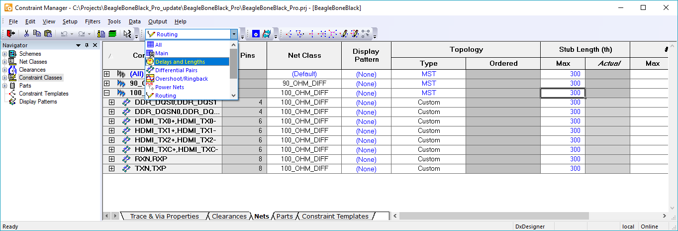
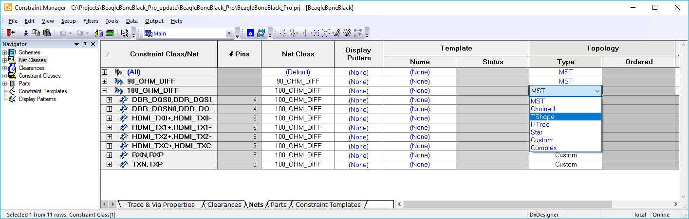
Topology constraints come in handy when routing particular nets. They are used to control the routing structure and can impose length restrictions. You may be able to find recommended topologies in datasheets to remove any guesswork in your design.
Many other constraints can be incorporated based on project type and requirements. Clearance constraints allow for a defined distance between routing objects. Differential pairs can also be constrained to specify separation distance, differential spacing, etc.
Although it is possible to create a full PCB without setting up constraints, taking the time to set up proper constraints early in the design process leaves minimal room for error when completing your project.
To get more details and tips for setting up constraints, check out this white paper: Eight Steps for Setting PCB Design Constraints Easily and Effectively.
Thanks for reading and see you next time for more on the ABCs of PCBs.
-Shivani Joshi