ABCs of PCBs – B for Board Layout
Welcome to ABCs for PCBs – a blog series to help new engineers learn about the world of Printed Circuit Boards. I’ll be covering topics from general engineering concepts to PCB design specific rules. As this is a ‘basics’ blog, I’ll keep the content software independent, but any visuals will be from the Mentors PADS Professional PCB suite.
If you missed the last post in this series: ABCs of PCBs – A for Analysis click here!
You’ve had a great idea for a project, you’ve created a schematic, and now it’s time for you to place your components and layout your board. You could just throw the components on randomly and hope for the best, but is that really the most effective procedure? The space allotted, location of certain parts, stack-up assignments, etc. all play a crucial part in overall cost and performance of the board. In order to keep things efficient, here are some tips on what to keep in mind during board layout.
One of the first things to check on would be your manufacturer’s specs. If the manufacturer cannot accommodate for a certain stack-up or materials, you’ll want to know that before using them in your design. Being proactive here is key to making sure redesigns are minimized.

Adding a ground plane could be advantageous to your design, but understanding the need and type of ground is important. For a two layer board, consider adding a ground plane on the bottom routing layer in order to protect your board from electromagnetic interference (EMI). It’s important to note situations in which avoiding a ground plane is best – for example, near RF transmitters. Using a hatch pattern with stitching vias is also a valuable technique where you can connect planes on the top and bottom of a two-layer board. Balancing copper and plane distribution also helps to prevent board warpage. We’ll go deeper into the concept of grounding later in this series.
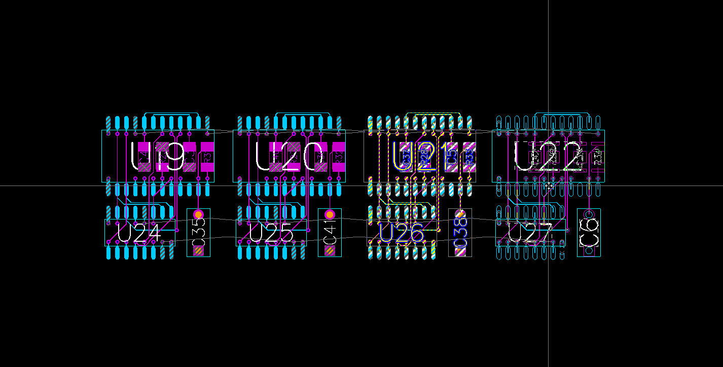
Component placement can be tricky on your first few boards, but there are a few techniques to keep things organized. Placing components (especially ICs) in the same orientation, will lead to fewer mistakes during assembly. Making sure the component land pattern is correct for your intended physical part is also crucial. Sometimes the datasheets, part manufacturers, or even the part you’ve downloaded or created may have mistakes or human errors. These can cause the wrong land pattern to be used and the issue may not be discovered until it’s too late.
The goal here is not to overwhelm, but to inform. Being proactive and cautious of potential board layout pitfalls can make your full PCB design process as smooth as possible.
Want to learn about advanced PCB design techniques? Check out this series: Layout automation using advanced PCB design techniques.
Thanks for reading and see you next time for more on the ABCs of PCBs.
-Shivani Joshi


