SerDes Design Part 6: JCOM, the Compliance Method for JESD204C Specification
Continuing my blog series on SerDes design, today we’ll talk about JESD COM (JCOM), a newly developed variant of Channel Operating Margin (COM).
JCOM has its origins in the IEEE 802.3bj COM revision and was created by the TG16 task group of the Joint Electron Device Engineering Council (JEDEC) as part of its JESD204C standardization work. To learn more about the IEEE 802.3bj spec, read part 5 of this series.
What is JCOM?
JCOM is the compliance methodology for high-speed serial links connecting analog-to-digital data converters (ADC) and digital-to-analog converters (DAC) to logic devices such as FPGAs or ASICS. Revision C of the JESD204 standard increases the maximum data rate from 12.5Gbps to 32Gbps and adds support for two additional link layers: 64B/66B and 64B/80B. The document designates six classes of links, grouped in two categories. Category B includes B-3, B-6, and B-12, each of them having a different maximum data rate. The three category C classes, C-S(hort), C-M(edium), and C-R(eflective) have the same maximum data rate of 32Gbps, but different minimum reference equalization architectures depending on the channel’s insertion loss characteristics. The transmitter, receiver, and channel compliance methodology for category C classes is based on JCOM.
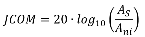
JCOM represents the signal-to-noise ratio (SNR) at the output of the receiver. It is calculated as the decibel ratio of the signal amplitude As over the noise amplitude Ani:
The JCOM reference model is similar to the one from the IEEE802.3bj standard for COM, except that the Tx and Rx device models are decoupled from the computational algorithm and the standard describes a mandatory interface to be used by the model developers to communicate with the algorithm.
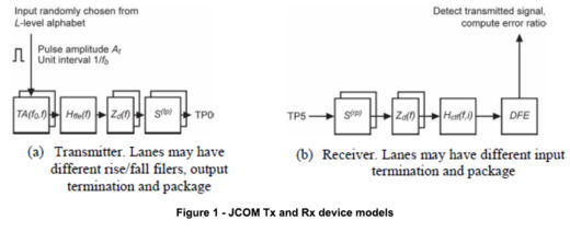
A new concept in JCOM is that of lanes which include device characteristics such as rise/fall time filters, terminations, and packages, as shown in Figure 1. For example, a transmitter might have multiple lanes with each lane having its own FFE, termination, package, and transition time adjust filter to set the corresponding rise/fall time at the transmitter output. Receivers may also have one or more lanes, each of them including a package, a termination, a continuous time linear equalizer (CTLE), and a decision feedback equalizer DFE. The reference models have three lanes. The channel is used for any combination of Tx and Rx lanes and consists of a victim signal path and any significant FEXT and NEXT aggressors.
Compared to the IEEE 802.3 COM, JCOM incorporates a number of improvements in the transceivers and package models. Among them is the modeling of the output/input impedances of the transceivers as frequency-dependent return loss as opposed to a constant resistance.
While the supplied Tx/Rx reference models can be used for interoperability testing purposes, just as they were in COM, JCOM has set the ambitious goal of increasing simulation accuracy by adding support for custom device and package models. Model makers have complete freedom in regard to package scattering parameters to be used in the simulations. The FFE, CTLE, and DFE are encapsulated in the device models and can report the number of available settings.
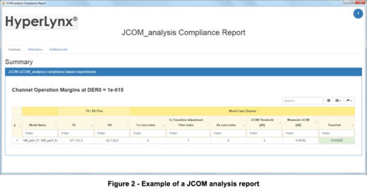
The computational algorithm is similar to the one from IEEE 802.3 COM, but the equalization optimization is performed for each possible combination of transmitter/receiver lanes and transmitter rise/fall times. JCOM is calculated as the minimum value resulting from all of those combinations, and it is compared to a 2dB threshold for channel compliance checking. Figure 2 shows an example of a JCOM report.
Despite the simplifications in the algorithms, COM and JCOM compliance methods offer several advantages when compared to frequency domain based metrics and IBIS-AMI simulations:
- They favor the trade-off between loss, reflections, crosstalk, and device specifications.
- They allow for solution-space exploration early in the design cycle, even if device -specific models are not available.
- They eliminate the intimidating complexities associated with IBIS-AMI simulations.
- They are faster, making COM/JCOM simulations more suitable for the post -layout screening phase of large designs
- They can be used to predict performance efficiently across high-volume manufacturing (HVM) tolerances with Polynomial Chaos Expansion (PCE) method and design of experiments (DOE) studies.
Read my article in Electronic Products to learn more about key aspects of the JESD204C standard as they relate to the channel-compliance methodology. Also of interest are Paul Dempsey’s article, How Channel Operating Margin Helps Gigabit Ethernet PCB Analysis, and BER and COM Channel Compliance, a DesignCon Best Paper award winner.


Comments
Leave a Reply
You must be logged in to post a comment.
I have one question.
If this SERDES line is operating as 16.22016Gbps, should I set the Bit Rate in “SerDes Wizard – Compliance Mode”
Yes and you can do that from within the Compliance Parameter Editor (“Edit Parameters” button in the JEDEC Channel Operating Margin page of the wizard). The signal rate is denoted by the f_b parameter (the first in the table).