Where Are All the PCBs?
 My grandparents asked me what I did once, and I had to explain to them what a PCB is. Being at their house with somewhat limited technology, it was rather difficult without having something to point to. So I decided I would bring one that I had lying around my house to show them. At the time, I pointed out that PCBs were in many different items in their home, including the hearing aids they were wearing. As you might imagine though, I wasn’t really willing to tear apart any of the devices they owned to actually show them a PCB.
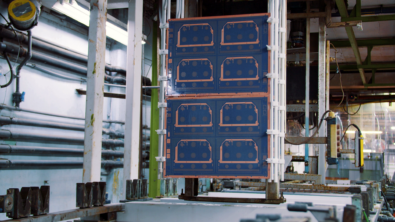
If you couldn’t go online and search for PCB images, where would you find a PCB in the real world to show someone? I had one at home left over from a project that I could show my grandparents, but it is an interesting question. These days PCBs are in many everyday things. The problem I had in the moment was that most PCBs are part of a larger design, and they are usually concealed from the user by an enclosure of some kind.
This highlighted to me the importance of electrical and mechanical domains working together during product design. Growing up, much to my parents’ dismay, I used to be able to disassemble anything with a Phillips head screwdriver, and quickly get to the “guts” of a device. Today’s more advanced designs require special screwdrivers and prying tools to coax apart the enclosure of a design to access the PCBs inside.
Although some designs can still be disassembled with a Phillips head screwdriver, even the designers of those boards need to know where the mounting holes for the enclosure will be located. For example, more-advanced designs might require that parts beyond a particular height not be in certain areas of the board due to tight physical clearances.
With device sizes shrinking as new versions of products come out, designers need to adhere to ever-tighter physical constraints, which means that PCB designers and mechanical designers need to collaborate more than ever before.
If you haven’t heard, the PADS MCAD Collaborator is available for free to PADS Standard, Standard Plus, and Professional users with the VX.2.3 version of PADS. This tool assists PADS users by communicating with a variety of MCAD tools, allowing both sides of the product design team to propose, accept, and reject changes to the design during the design process. I did a web seminar on this recently called Collaborate to Overcome Electro-Mechanical Design Issues. Why not check it out?


Comments
Leave a Reply
You must be logged in to post a comment.
A few decades ago I used PADS PCB (DOS based) to design some nice PCBs including SMT designs. I still have the install diskettes somewhere, but they are waaaay out of date. I wonder if there is an upgrade path? :>)