What causes undesirable SI in DDR designs?
 Continuing my blog series on DDR [Part 1 – Controlling DDR, Part 2 – Memory Bus Basics, Part 3 – Data Bus Basics], this post briefly reviews some of the common causes of undesirable Signal Integrity (SI) effects in DDR designs.
In general, there are three sources of undesirable SI effects: 1) the Transmitter; 2) the Channel; and/or 3) the Receiver. Of the three, the PCB designer has the most control over the Channel itself.
IC vendors
The Transmitter and the Receiver are largely defined by the IC vendors. There might be different drive strength options, and different slew rates that the IC vendor offers for the chip when it is driving. Similarly, the IC vendor may offer different On Die Termination (ODT) options when the IC is receiving. The best signal integrity quality can be achieved for a system by matching the Transmitter and Receiver behavior to the characteristics of the channel. The Transmitter and Receiver behavior is set in an actual system by means of programming registers on the device. In simulation, behavior is set by selecting the buffer model corresponding to the driver/receiver option to be tested.
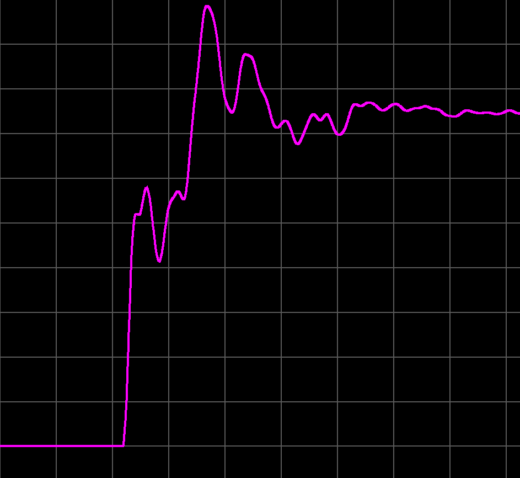
While the specific setup needs to be simulated to gain accurate insight to the behavior of the system, as a general rule of thumb you can assume that strong transmitters and weak ODT receivers will cause more overshoot and undershoot ringing, while weak transmitters and strong ODT receivers might prevent the signal from reaching the desired high/low threshold states if run at high frequencies.
Recommendations for PCB designers: two scenarios
Though setting the Transmitter and Receiver behavior is important for getting a system with good SI, the board designer usually has the most control over the PCB itself. Here, we can discuss the channel characteristics of the Data (including strobe) lines and the Address (including clock) lines.
The Data lines are likely to be point-to-point for most embedded designs. In this case, one end of each data signal will be at the controller and the other end at the DRAM. During Write transactions, the controller is the transmitter with the DRAM as the Receiver. During Reads, the roles reverse. SI should usually be pretty robust in these designs.
To optimize SI, design considerations (in addition to general SI layout considerations) for this case are:
- Minimizing the number of layer transitions to minimize vias and their stubs
- Selecting the appropriate Transmitter and Receiver models for both the controller and DRAM
- Minimizing the length of the channel
- Minimizing the skews between the signals of each lane.
In a Multi-Rank setup, each data signal can have multiple DRAM drops. In this case, the segment from the first DRAM to the second can behave as an undesired stub when transactions are taking place between the controller and the first DRAM. So, the selection of the ODT behavior when accessing each DRAM needs to be more carefully analyzed. For example in a two-rank setup, when the controller writes to the nearby DRAM, the SI at that DRAM is crucial. When the DRAM at the farther DRAM is written to, the SI at this location becomes crucial. So, the optimal ODT settings might change based on which rank is being accessed. This can be analyzed in simulation.
The Address bus for DDR3 onwards is laid out in a fly-by topology. In this case, the signal is terminated only at the end of the address bus, and there are likely to be reflecting effects for each of the DRAMs which are farther away from the terminating resistor. Since the SI due to these reflections is worse than in the data bus, the address bus is usually run in Single Data Rate, or sampled only on the rising clock edges. In this case, in addition to general SI guidelines, it is beneficial to:
- Minimize the length of the channel between the first and the last DRAMs
- Minimize the length from the last DRAM to the terminating resistors
In the next blog, we will discuss the requirements usually set by the controller and the DRAMs.