Designing PCB’s for IoT – Part 1: IoT Everywhere
A recent IHS report forecasted that the IoT market will grow from an installed base of 15.4 billion devices in 2015 to 30.7 billion devices in 2020 and to 75.4 billion by 2025. (Source: IoT platforms: enabling the Internet of Things, March 2016 ) This forecasted growth translates to a potential economic impact of 2.7 to 6.2 trillion USD. So, ready or not, here comes IoT and in a big way.
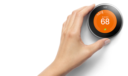
Nest® thermostat
IoT enabled products and devices including fitness trackers, smartphones and household devices are becoming more and more a part of our every day lives. However, IoT technology goes far beyond mainstream consumer devices. From advanced medical devices to sensors used in factory automation, industrial robotics, agriculture, automotive, road and railway transportation monitoring to water distribution and electrical transmission, IoT technology is quickly propelling humankind into an IoE (Internet of Everything) world.
The printed circuit boards we design for IoT devices are unique because they present a distinct set of design challenges. They are characterized by compact form-factors, high-speed processing, multi-mode support and integrated Wi-Fi and Bluetooth. low energy, storage and memory must also be considered.
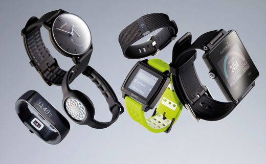
A selection of wearable fitness trackers
IoT product development isn’t limited only to big companies that develop mass consumer products. In fact, the accessability of today’s IoT platforms have lowered the barriers to entry for inventors, Makers and entrepreneurs to develop and rapidly prototype new IoT products. The opportunity for a Maker for example to invent a new product, get exposure and raise money from crowdfunding sites exceeded $34 billion USD in 2015, surpassing VC investments.
Part 2 of this Designing the PCB’s for IoT blog series will focus on the domains of IoT design. To learn more download my white paper: 7 Design Aspects of IoT PCB Designs.
Thanks for reading!
John