The PCB Design Ecosystem = Unified Tools
Access to design IP and collaboration is key to meeting the needs of engineers in the electronics product design ecosystem.
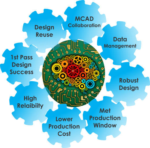
Managing the ecosystem from within a unified design tool enables engineers and PCB designers to leverage design IP with the final product in mind, analyzing and validating each aspect, effect, and impact encountered along the way. From part selection, design reuse, simulation, and early collaboration with MCAD, the design ecosystem can ensure end-product success.
This short excerpt from my recent article published in EP&T – Electronics Products and Technology, read the full article here: https://issuu.com/glaciermedia/docs/ept2016may01/20 highlights how access to design IP and collaboration is key to meeting the needs of engineers in electronics product design in today’s PCB design ecosystem.
Learn more about the PADS Product Creation Platform
Thanks for reading, John