5 Key Advantages of 3D PCB Layout
Having a 3D view in PCB design tools is not new. However, 3D capabilities have greatly evolved over the past five years or so. What was once a “nicety” is now vital to the PCB design work environment.
3D is becoming the layout environment of choice. It provides views of both electrical and mechanical 3D models, which display a virtual prototype of the finished PCB assembly within its enclosure, that a 2D layout environment can’t.
5 Key Advantages of a 3D Environment for PCB Layout
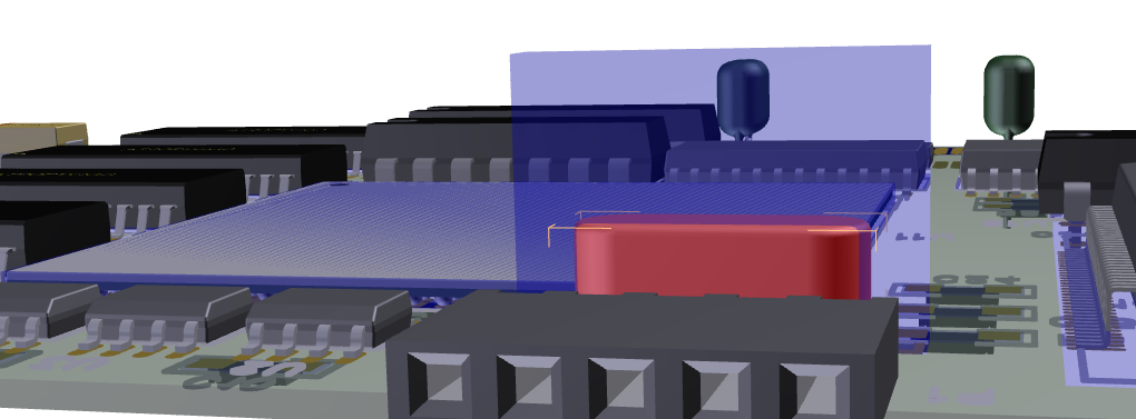
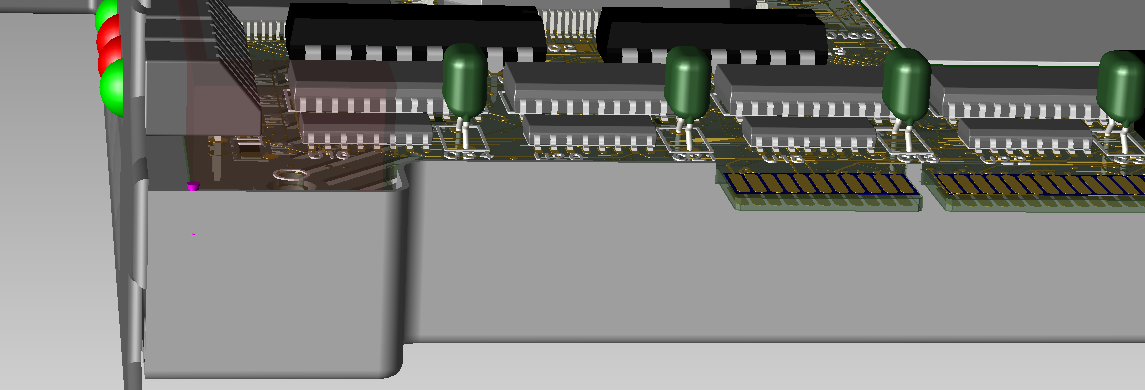
1. Placing accurate component models in 3D gives designers immediate visual feedback.
One example of this feedback is being able to detect shadowing concerns for tall components that may impact wave soldering. From tall pin headers used for mounting daughter or mezzanine cards, to SIMM and CPU sockets, 3D visualization brings component placement into a new era.
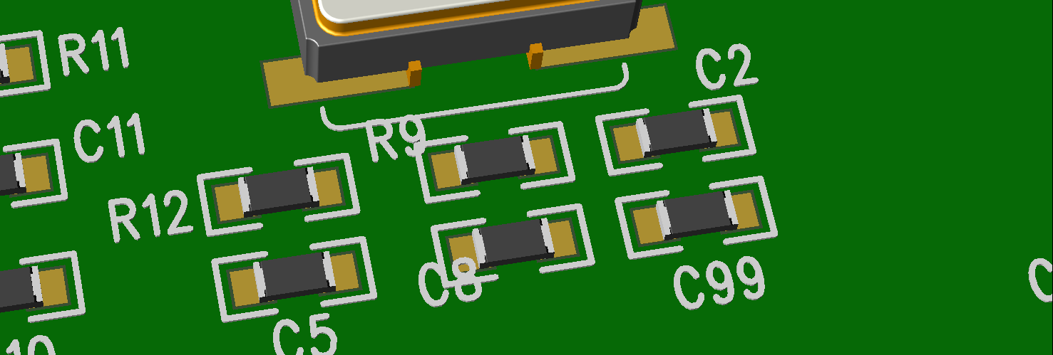
2. With accurate 3D models, the component silkscreen outlines and reference designators can be placed more accurately.
Make sure component bodies do not inadvertently overlap reference designators and discover when they are accidentally placed overlapping solder mask clearances. Photo-realistic 3D views enable design teams to review the PCB artwork from a whole new perspective.
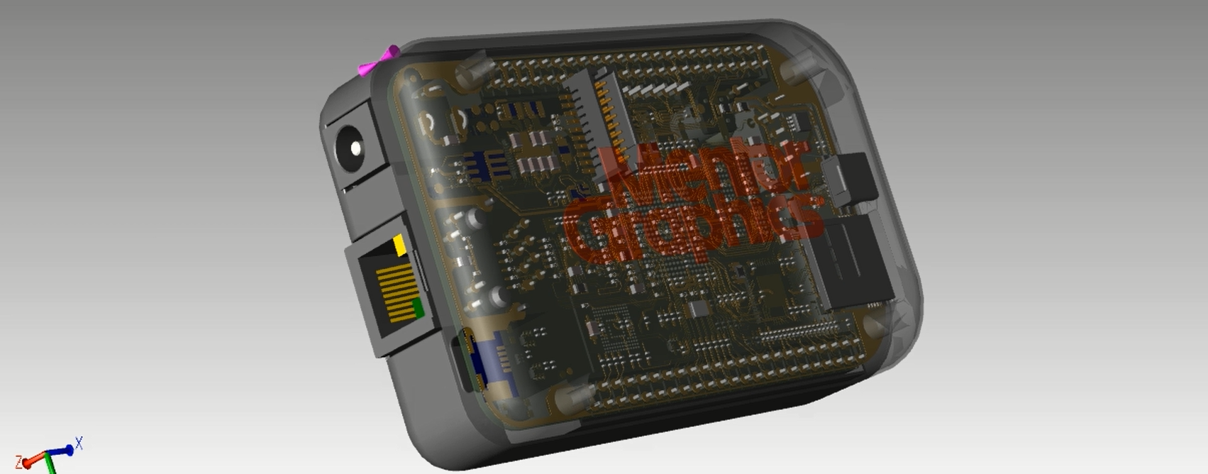
3. Incorporating 3D models of the mounting hardware including screws, washers, and standoffs helps ensure that there are no surprises when it comes time to mount the PCB.
You may discover a mounting hole that should have been plated for a chassis ground connection. Or, perhaps you’ve detected that the BOM’s chosen flat washer overlaps a trace in time to correct it by either moving the trace(s) or by changing the part on the BOM to a washer with a smaller OD. The ability to incorporate mechanical hardware, and even be able to try different styles of fasteners in the 3D layout adds a new dimension to PCB design and MCAD collaboration.
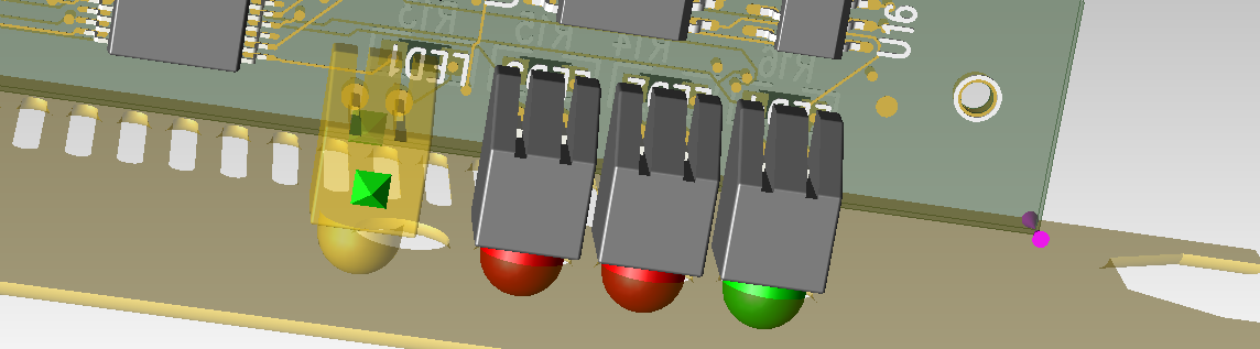
4. Validate physical interface components.
We’ve all seen SMT connectors that have the same land pattern for both male and female versions. Bringing in the actual component models for connectors, headers, LEDs, switches, etc. can help to ensure that there are no unexpected surprises during assembly. Even mating connectors can be included to ensure that no interferences with the PCB components are detected when connectors housing are bulky, or if they include latching mechanisms.
5. Enclosures and mechanical piece parts like brackets, board stiffeners, and RF shields, for example, can all be imported to insure that the necessary clearances are met.
From making sure correct solder mask clearances are correct to preventing shorts when mechanical items are mounted, knowing that everything from the PCB sub-assembly to its installation will work correctly the first time is priceless.
Click here to learn more about 3D PCB layout in PADS.
Thanks for reading,
John


Comments
Leave a Reply
You must be logged in to post a comment.
It’s a very nice new design. 3D avoid any mistake of designer.