Behind the Design: Fujitsu Technology Solutions GmbH
This is the sixth post in a series showcasing the winners of the 2014 Technology Leadership Awards. View the previous ones here.
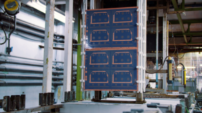
First place winner in the Industrial Control, Instrumentation & Medical category: Fujitsu Technology Solutions, Germany
![]()
Design: A biometric multi-factor authentication; a flexible high-security platform solution for access control, payment terminals, and match on device. The system is based on ARM SoC with crypto co-processors.
Design team: Andreas Schaefer, Timo Bruderek, Joachim Bub, Andreas Titz, Willi Neukam, Peter Bräu, Werner Hasubick, Rudi Häußermann, George Emanuel Valceanu
Design challenges:
- Security certification: We had to protect the PCB physically against access and intrusion (shield sensitive signals on internal layers with a unique via scheme), and manually routed patterns using a 3-2-3 HDI stack-up.
- Electro-mechanical design: Spent a lot of time synchronizing with MCAD team on the housing construction.
- Rigid-flex, RF technology.
- Some high-speed due to DDR3, Ethernet and USB
- Tight placement: Lots of mechanical components, some with through-mounts that had to avoid parts on the opposite side.
- ARM CPU: 100% connected, associated passives and test points were placed on reverse side, 7 power rails.
- Panelization: Concern for SMD components on the edge; the contour on one side didn’t allow standard V-cuts.
- We took on a new fabrication process that required optimizing the process from design through manufacture.

Design tools and team comments:
- Xpedition Enterprise (New VX.1 Release)
- “Used 3D integrated layout to ensure that component placement didn’t collide with the display housing. This combination of PCB optimization and mechanical part fittings can be found everywhere and would have been impossible without the 3D layout feature. The new 3D layout placement and online DRC capabilities were used heavily during this design. With the use of simultaneous 2D and 3D placement control, we achieved very good mechanical accuracy for the first prototype. This quality and accuracy has only been seen in the second or later prototype stages for past projects. We saved approximately 12 weeks by eliminating prototype cycles.”
- “Accurate 3D models were required; rough 3D models and 2D obstructs were insufficient.”
- “The design was completed in 8 weeks. The team successfully developed the product while they also implemented new design software, created a new library, and transitioned to new board technologies.”
Judge’s comments:
- “A high-density flex-rigid design showing the best of design density, advanced manufacturing technology, and flex.”
- “A Complex 3D problem with interesting methods to manage security of circuit.”
- “Good stack-up on a tight board.”
- “Very detailed descriptions of the issues they had to overcome to produce a very tight board. I like the way they utilized the various tools to achieve design requirements.”
About the Technology Leadership Awards
Started in 1988, this program is the longest running competition of its kind in the electronic design automation (EDA) industry. It recognizes engineers and designers who use innovative methods and design tools to address today’s complex PCB systems design challenges and produce industry-leading products. See the full list of 2014 winners here.