The Myth of the Pretty Design
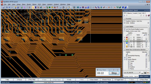
 I often talk with friends and colleagues in the PCB design community about trends. A subject that comes up often, and has probably been beaten to death, is the use of auto routers in today’s PCB designs. The answer I hear more often than anything else is, “We don’t use auto routing on our designs.” Why is this?
Is there something that auto routers are not providing? Is there something more they could do? Are they not fast enough?
I often hear, “I don’t like the way they route.” It’s true, X/Y layer biasing and lots of vias placed can make for a lot of manual cleanup. Maybe this is why I also get the comment, “I like my designs to be pretty.”
Please continue reading after you stop nodding your head or laughing…
The myth of the pretty design is just that, a myth. Hand-routed designs do not work better than an auto-routed design, as long as all of the rules are adhered to. Auto active routing creates quality designs through shape based, correct-by-construction rules, whether auto or by hand. So where is the happy medium that will make us more effective designers, instead of glorified digitizers of endless numbers of vertices? Do auto routers need to get better? Or, does interactive routing need to supply more forethought as we lay in etch?
Take a look at this webinar and we will discuss the future of routing technology further in upcoming posts within this series. In the meantime, share your thoughts on this subject in the comments.
Routing Automation: A Breakthrough in Productivity
Comments
Leave a Reply
You must be logged in to post a comment.


It’s easy to see where we are headed. Manually directed routing with an assist from a powerful auto active engine in the background. I expect to be able to move from circuit to circuit laying in etch with the twists worked out as I go. Nice!
At first i do not like auto routing, only to found out that I myself do not have the system to implement it step-by-step..Today, I found auto routing is one of the remarkable breakthrough in design Productivity. But it requires good planning. every design have own way of attacking the designs, and it varies depends on how small or big the projects. Hopefully You could add features on power sketching plan. This one of main challenge during the post design. A lot of designers advanced the design with great speed during signal wiring,, and redo their work due to weak power routing.
I have been out of the business for 12 years (retired) and just for grins I thought to go to your site to see what’s up. My career was with AT&T/Lucent and 2 years with Plexus. I had to chuckle when I saw the titles of your articles. In a nut shell, the more things change, the more they stay the same!! Interaction with your EE is critical to understand objectives and requirements. I felt component placement was the KEY building block to a successful design. Also I would spend considerable time with building fanouts around components, using both autorouter and manual routing. Diligent fanout building resulted in more successful auto routing runs (typically from mid to high 90% connectivity results). A big help was AT&T/Lucent being a beta site and we had the resources to staff an EDA team creating custom software tools. One thing I would disagree with you would be laying out a “pretty” design. I strongly believed a design that looks “pretty” fabricates and performs better. Thanks for taking the time to read the ramblings of an old fart!