The PCB Design Flow of the Future
Back in the mid-80’s when I first started hand-taping PCB designs 2:1 on mylar, it was pretty clear that printed circuit design wasn’t a simple start-here-and-proceed-to-the-finish-line type of design flow. Design changes happen. Getting a new netlist with a re-pinned out FPGA just after you’ve finished routing a design is not a new anomaly. Just try to imagine how big of a pain it was and how time-consuming it used to be to rip-up and re-tape every layer for design changes.
Fast forward to 2014, PCB designs are still not immune to design changes. Depending on your PCB design flow, hand-offs from one phase of the design to another are not always predictable or necessarily smooth. The reality is there are a lot more steps involved in the PCB design flow today. Sure, some changes are smaller and less impactful, but others require lots of rework and can be very time consuming, especially with the compact, high-speed, highly constrained, mixed-technology designs we take on today. Areas of the design that the ECAD engineer interacts with today span several, if not most, of the phases illustrated in Figure 1.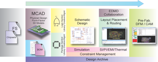
Figure 1
Perhaps this flow looks familiar. The question is, how do we make it better? Can/should the order be less linear so that different phases can be worked-on simultaneously? The answer is yes.
Trends in modern PCB design make it possible to access and accomplish different tasks throughout the design flow. For Example, Figure 2 depicts many of the ways that PADS has evolved into a modern, integrated design system that provides integrated functionality throughout the design process.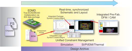
Figure 2
The new PADS integrated PCB design flow depicted in Figure 2 focuses on removing disconnects and error-prone file and data transfers that occur with disjointed or traditional linear PCB design flows. This database-aware flow ensures that coherency of the design’s logical, physical and constraint data is synchronized.
Key features and advantages that the new PADS integrated project provides are:
- Direct access to component databases with parametric search engine capabilities enabling users to locate parts and manage both logic and physical symbols.
- Direct link from your project to one central library that ensures library data consistency is maintained.
- Integrated analysis and verification tools for circuit design, simulation and signal integrity planning.
- Direct, synchronized connection between Schematic and Layout, including automated back-annotation of connectivity changes made in Layout.
- Integrated constraint management and verification throughout Schematic Capture, Layout and Routing.
- Real-time bi-directional ECAD/MCAD collaboration through the industry standard ProSTEP iVIP IDX file exchange.
- Integrated DFM fabrication and assembly analyses identify production issues prior to fabrication.
- Archive management system that enables users to store and restore the complete design project.
Even with all these advantages of a modern integrated PCB design flow, as I stated earlier design changes happen. However, by utilizing an integrated and synchronized design flow you can shorten the design cycle and reduce the impact on both time and cost of design changes.
You can learn more about the PADS integrated flow by watching this on-demand Webinar: Shorten PCB design time with PADS real-time data synchronization and integration
Thanks for reading !
John