PCB and Routing Solutions: Centering Traces in BGA
This is the second post in this routing series. View the introduction post here.
To increase fabrication yield, it is important to center the traces between the fanout vias inside the BGA area. Large BGAs are usually 1mm pitch and medium sized ones are 0.8mm. Then we go down to 0.65, 0.5, 0.45 and 0.4. Is anybody designing with even finer pitch BGAs?
In any case, it is important to center the traces between the ball pads and/or the fanout vias. If the routing is on the outer layers, then it is important that the traces do not get exposed with the soldermask openings. Of course, if the BGA pads are soldermask defined, then the problem of exposure is eliminated; however, this method is not always used.
On inner layers, any increase in the via-to-trace spacing will help to prevent shorts during the fabrication process. When fabricating boards, “Spacing is King.” You may also want to force the traces to be centered so they will not cross anti-pads on the plane adjacent to the signal routing.
Difficulties include various pin pitches, and we also have to deal with differential pairs along with the single-ended routing. As the pin pitches vary, rule areas can accommodate finer trace widths and spacing, and if set just right, it can automatically force either the differential pairs or individual traces to be centered. The problem is with “either.” If both differential pairs and individual traces need to be centered, a single spacing value will not force all the traces to be centered.
There is a method in existing Expedition PCB and Xpedition Layout that can be used to accommodate the centering of both single ended nets and differential pairs.
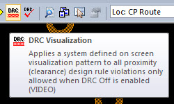
Solution: DRC Visualization and Repair
The step-by-step instructions are as follows:
1. Differential Pairs: In the Constraint Manager, increase the trace-to-via (or if on the mount layer, trace-to-pad) clearance to a value so that the differential signal will be centered. You can do this in the default rules, and if you are using rule areas around the BGA, you can do this for each of the rule areas. I trust you can do the math.
2.Turn on visibility of all routing layers. Run the DRC Visualization routine.
3. There is no need to look at all the violations – there will be many. After the DRC completes, select the traces you want to have centered, and click the right mouse button.
This menu will appear:
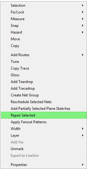
4. Choose “Repair Selected” and all the DRC violations that can be repaired will be repaired by pushing the traces away from the pads and vias.
5. Set your Gloss to “Local Gloss,” frame-select the traces that you just repaired, and then choose “Gloss.” This will remove any small segments that might have been created.
6. Do this method for all the BGAs that have differential pairs running through them.
7. Set the trace-to-via and trace-to-pad clearances back to the original values. You can also accomplish this by exporting the original constraints and then importing them back into the design.
8. Single-Ended-Nets: After the differential pairs have been centered, go through the same cycle with single-ended-nets. The differential pairs will not be affected by this operation for single-ended nets.
9. Once the rules are reset to the original rules, do a full DRC to ensure that no other problems may exist or have been created during this centering process.
At this point, the vast majority of the traces will be centered as desired. It may read like a lot of steps, however, it is certainly much more effective than centering the traces manually.
Here is a video that illustrates centering of differential pairs.
Are there other methods that you would like to offer?


Comments
Leave a Reply
You must be logged in to post a comment.
Really good stuff Charles! I’m just surprised that you haven’t engineered this into Xpedition yet. There was something like this in SuperMax, so… how hard can it be to fix this?? 🙂
@Bengt – For now, this method shown above works the best. If our customers would vote for a general centering capability on Mentor Ideas, it could get a higher priority.
https://na5.brightidea.com/ct/s.bix?c=E411B1F9-EB21-43A6-A2C9-1A23CBDF3E95
Nicely done! I have always felt that the you know you have great software when you can manipulate it to do things beyond its original intent.