When Dummies Turn Smart: The Evolution of Dummy Fill in Advanced Semiconductor Manufacturing

Yield stands as a critical performance indicator in semiconductor fabrication. Higher yield rates reflect optimized manufacturing processes that produce functional chips, directly translating to improved profitability. Conversely, lower yields indicate process deficiencies, resulting in defective chips and significant financial losses.
Integrated circuits are built layer by layer, much like constructing a multi-story building. For each new layer, the surface below needs to be perfectly flat, just as a building needs a level foundation for the next floor. This flattening process, called planarization, is done in semiconductor foundries using special machines called Chemical-Mechanical Polishing (CMP) machines.
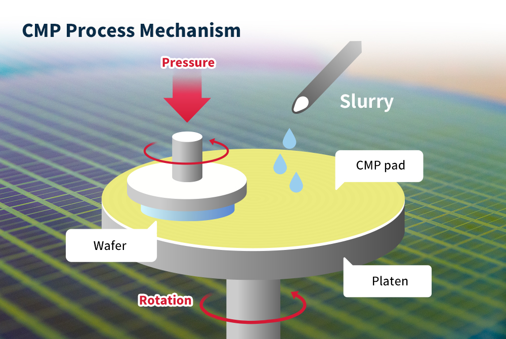
For CMP machines to work best, the chip surface needs to have a consistent density. However, chip designs often only use certain areas, leaving many spots empty. For example, a “Metal1” layer might only be in specific regions, leaving large areas without any metal. To help the CMP machines work effectively, designers add extra metal shapes to these empty spaces. These added structures, which don’t have any electrical function, are called “dummy fill.”
In mature technology nodes, dummy fill insertion was straightforward, with minimal impact on circuit performance—they were truly “dummy” elements. However, as the industry has progressed toward advanced nano-scale and sub-nanometer nodes, these once-passive structures have begun to influence design performance significantly. This paradigm shift necessitates sophisticated, carefully engineered approaches to dummy fill insertion. This evolution marks the transformation where “Dummies turn Smart”—requiring intelligent placement strategies that balance manufacturing requirements with electrical performance considerations.
Intelligent placement strategies encompass a range of sophisticated techniques designed to address the complex challenges of advanced node manufacturing. One critical approach involves positioning specific geometries adjacent to signal lines to mitigate Optical Proximity Correction (OPC) issues—a technique known as OPC Fill. Beyond optical considerations, advanced fill structures are engineered to minimize parasitic capacitance effects while simultaneously enhancing thermal dissipation across the design.

Siemens Consulting plays a pivotal role in delivering these advanced solutions through our dedicated Yield Enhancement Services (YES) team. As a specialized division within Siemens EDA, YES provides expert consulting services that leverage the industry-leading Calibre SmartFill engine. This team works closely with semiconductor manufacturers to develop and deploy customized algorithms tailored to their specific process requirements and design challenges. Through this collaborative approach, Siemens Consulting enables intelligent placement strategies that ensure dummy fill structures not only satisfy manufacturing constraints but also optimize electrical performance and thermal management—ultimately delivering measurable yield improvements and competitive advantages for clients working at the cutting edge of semiconductor technology.
For more information on using Siemens Consulting to accelerate the productivity of your Calibre flow, talk to your local Siemens representative or contact us here!
Authors:
Haitham Eissa, Consulting Solutions Architect Fellow, CLS Yield Enhancement Services
Amr Khafagy, Principal Consulting Solutions Architect, CLS Yield Enhancement Services