Stop tracing nets by hand, start seeing them
You’re deep in a design review when something doesn’t add up, a net you’re sure is connected to one block doesn’t seem to behave that way. You start clicking through the schematic or scrolling through a layout with thousands of interconnected shapes, trying to manually retrace the path. It’s slow and it’s easy to miss a subtle connection along the way.
By the end of this post, you’ll know how to see full net connectivity directly in your schematic and in your layout, without digging through documentation or waiting on extraction.
When connectivity is hard to see
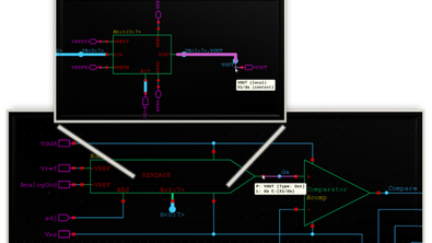
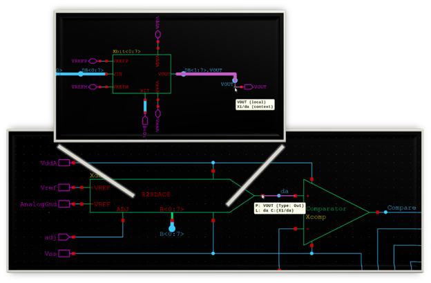
In a schematic, a net’s name can change at every level of the hierarchy. A digital-to-analog converter (DAC) output might be named Vout locally, da one level up and X1/da by the time the simulator reports it, reflecting the hierarchical path through that instance. It’s still one continuous net but confirming that requires tracking how the name resolves across each level.
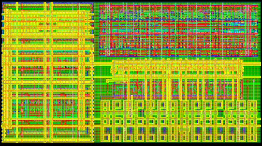
The problem takes a different shape in layout. There, connectivity is about geometry, not simply naming, metal layers connect through vias, diffusion and polysilicon connect through middle-of-line (MEOL) layers and some processes include multi-patterning and cut metals that further introduce complexity. In a dense layout with thousands of interconnected shapes, manually tracing connectivity is tedious and prone to human error. A subtle connection or a layer transition can be easy to miss.
Why manual tracing breaks down
In a hierarchical schematic, the simulator resolves a net’s many local names down to a single, consistent name, typically the one from the highest level of the hierarchy, known as the context name or alias. That resolution happens inside the simulator, but reading a schematic doesn’t automatically show you that mapping.
In layout, the application is different: connectivity rules are defined by the process design kit (PDK) and vary by layer type and patterning scheme. Manually configuring those rules for each new design wastes time, and misconfigured rules lead to incorrect results, errors you might not catch until it’s too late. Post-layout extraction tools help, but they require time and setup you don’t always have during active design iteration.
See the connection, without waiting
Two separate capabilities in our tools address this, one for the schematic, one for the layout, each making connectivity visible directly where you’re working, instead of requiring a separate lookup or an extraction run.
Step 1: Hover to see the full net instantly (in the schematic)
S-Edit’s Dynamic Info highlights every segment of a net as you move the cursor over it and displays a tooltip showing both its local name and its context name, the name the simulator uses across the whole hierarchy. For nets connected “by name” rather than by a drawn wire, Dynamic Info draws arcs between the connected parts, so the relationship is visible immediately instead of implied. This matters because it removes the need to manually track how a net’s name changes from one hierarchy level to the next.
Step 2: Pull the exact detail you need (in the schematic)
The same tooltip surfaces information not otherwise visible on the schematic, which implementation view is active for an instance (for example, an analog SPICE model, a Verilog-A behavioral model, or a digital Verilog model, useful in mixed-signal simulations), the full hierarchical path to the instance, and default values for global ports or inherited connections. Additionally, this capability is available without permanently taking additional screen real estate often found with other tools. When you need that information elsewhere, pressing A while a tooltip is visible sends its text to the command line and copies it to the clipboard automatically. This matters because it turns information you can see into information you can immediately reuse.
Step 3: Confirm it in the layout, without waiting for extraction
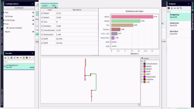
The L-Edit Highlight Connected feature reads connectivity rules directly from the PDK including vias, MEOL layers and multi-patterning, with no manual configuration needed. Select any shape and the entire connected net is computed and highlighted immediately, cascading through every level of the design hierarchy. For massive nets, you can control the pace by defining a number of iterations or a time duration and you can pause or interrupt the highlighting at any point to see what has been computed so far. This matters because it gives you the same on-demand visibility in layout that the schematic already provides, without an extraction step.
Takeaway
Before your next design review, it’s worth checking:
- Can I confirm a net’s name across every hierarchy level without manually tracking each change?
- Do I know which connectivity rules apply to this layer stack, vias, MEOL, multi-patterning, without configuring them by hand?
- If a net is large, can I control how much of it I see at once, rather than waiting for the full computation to finish?
If any of those require extra steps today, that’s time spent on manual tracing that these two capabilities are built to remove, one in the schematic, one in the layout.
Watch the S-Edit Dynamic Info YouTube video to see the hierarchy tracing and tooltip details from Steps 1 and 2 in motion. Then watch the Highlight Connected demo to see Step 3 in action, tracing a live net across a layout without waiting on extraction.
Authored by Custom IC Design Team