Driving 3D IC innovation with Calibre multiphysics

By John Ferguson
Here’s a surprising truth: the idea of 3D integrated circuits (3D ICs) isn’t new! It traces back to the 1960s, right after the MOS IC was first proposed, and by 1983 Fujitsu had already demonstrated a TSV-based 3D CMOS stack using laser beam recrystallization.
Yet, only now has the industry finally unlocked the true potential of 3D integration after decades of innovations in design, packaging, and manufacturing. The global 3D IC market is projected to soar to $51.81 billion by 2030 with a CAGR of 20%.
By vertically integrating heterogenous chiplets, 3D ICs deliver significant gains in performance, functionality, and energy efficiency for AI accelerators, HPC systems, and mobile devices.
But this leap forward also introduces new challenges. Multiphysics interactions and system reliability issues make a holistic design approach essential.
All physics is “multiphysics”
You’ve probably heard this one before: an object at rest stays at rest, and an object in motion stays in motion—unless acted on by an external force. That’s Sir Isaac Newton’s Law of Motion.
What we often overlook is the key phrase: “external force.” In the real world, those forces are everywhere—gravity, friction, heat, electrical charge, pressure, sound waves, and more. And none of them exist in isolation.
A shift in temperature can alter pressure, trigger condensation, or generate wind. We try hard to isolate these forces when possible, but it’s never entirely achievable. This leads us to Sir Isaac Newton’s Second Law of Thermodynamics, the Law of Entropy.
In short, all physics is multiphysics!

Multiphysics problems every 3D IC designer must solve
The shift from 2D to 3D ICs fundamentally alters the design environment and amplifies the need for early multiphysics analysis. Below are two key challenges amplifying the need for early multiphysics analysis.
Heterogeneous integration introduces new uncertainties
In 2D SoCs, engineers rely on mature PDKs, predictable workflows, and standardized signoff processes. Thermal and mechanical checks can often be deferred until late in the cycle with minimal risk.
In contrast, 3D integration breaks these assumptions. Stacked architecture often combines heterogeneous dies built on different process nodes, material stacks, and interconnect technologies. TSVs, micro-bumps, hybrid bonding layers, and advanced packaging structures all introduce new sources of variability.
A modern 3D IC may contain billions of components embedded within complex packaging materials, creating a tightly coupled system where multiphysics effects are far less predictable than in 2D.
Tight coupling of heat, stress, and electrical behavior cause troublesome errors
In a stacked architecture, multiphysics effects become significantly more pronounced. Delivering power through multiple dies increases current flow—and therefore heat. That heat affects transistor behavior, timing closure, and electromigration. Because heat now must travel through stacked layers before escaping to the heat sink, it dissipates more slowly than in 2D designs.
Meanwhile, different materials in the stack expand at different rates, creating thermomechanical stress that can lead to misalignment or warpage. If these thermal issues go unaddressed, they can quickly cascade into signal-integrity problems, timing failures, reliability degradation, or structural deformation.
New design paradigms required for 3D IC success
3D IC requires designers to adopt three philosophies.
Number 1: Shift-left or fall behind, multiphysics must start early
In traditional 2D SoC development, many key physical assumptions are fixed early at the RTL stage. Timing corners, power models, and basic thermal envelopes are defined upfront, with detailed thermal and mechanical checks performed late in the flow—usually with a manageable impact. In 3D ICs, such an approach is no longer viable.
A chiplet may operate within specifications in isolation yet face degraded reliability when exposed to the actual thermal gradients, stress fields, power-delivery impedance, and IR-drop profiles inside a 3D stack. These effects must be considered much earlier during architecture, chiplet partitioning, RTL modeling, and floorplanning.
Multiphysics evaluation must also be continuous through every design iteration. Each change to layout, interfaces, or materials can change thermal paths, stress patterns, and electrical parasitics, which must be re-validated to maintain reliability and yield.
Number 2: Break design silos away from the die to system centric
3D ICs require close coordination among specialized teams: die designers, interposer experts, packaging engineers, and, increasingly, electronic system architects and RTL developers. Yet each group often works in different toolchains, with different data models, naming conventions and coordinate systems, creating friction points that slow integration and introduce errors. This complexity multiplies when chiplets originate from different vendors, as they arrive with varied methodologies, abstractions, and data formats.
Addressing these disparities requires a system-level owner, supported by comprehensive EDA platforms that unify methodologies, aggregate data across domains, and enable a holistic view of the entire 3D assembly.
Number 3: Use predictive analysis to reduce thermal risks
The vertical proximity of active dies can lead to rapid heat accumulation and risks. For example, with thermal runaway, ongoing heat generation further degrades electrical performance and creates mechanical stress from varying thermal expansion rates in different materials. Differential expansion between materials can even warp dies and threaten the reliability of interconnects.
To enable predictive design, the industry needs standardized “multi-physics Liberty files” that define temperature and stress dependencies of chiplet blocks, akin to the Liberty files used for place-and-route in 2D design. These files would let designers verify whether a chiplet remains within safe operating limits under expected thermal conditions.
Multiphysics analysis must also enable back-annotation of temperature and stress into chiplet-level models, ensuring timing, EM, and IR-drop calculations reflect real operating environments.
EDA’s role: Evolving IC design to the system level
As 3D ICs push design to the full system level, EDA vendors play an increasingly critical role in enabling inclusive environments and seamless collaboration across fabless teams, foundries, and OSATs. Robust data exchange and interoperable toolchains are essential for clean handoffs, consistent system views, and traceable communication throughout the supply chain.
The industry is rapidly developing new standards and 3D IC design kits that define common formats for chiplet components, interfaces, and package architectures. Such initiatives enable reliable data exchanges and integration across diverse teams. For instance, programs such as TSMC’s 3Dblox provide upfront placement and interconnection definitions, reducing ambiguity, and fostering interoperability.
Streamline 3D IC design with Siemens
3D ICs redefine how design, verification, and manufacturing must work from the die to systems. That’s why we partner closely with TSMC and other ecosystem leaders to deliver a holistic, streamlined 3D IC workflow from concept and early planning through verification, tape-out, and manufacturing.
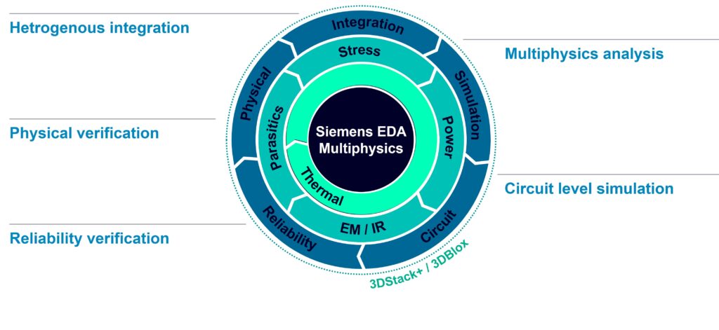
Transform isolated analyses into integrated, collaborative workflows
Whether validating heterogeneous assemblies or managing thermal threats from localized power densities, these challenges introduce new failure modes that cannot be captured by isolated verification approaches. Siemens has recognized these evolving needs and invested in building a cohesive, extensible 3D IC verification ecosystem.
Here are a few of Siemens’ latest innovations.
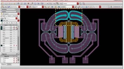
- Comprehensive 3D physical verification: With the growing influence of multiphysics effects, DRC and LVS checks must be performed with additional analyses of thermal and stress domains, providing a holistic view of risks and performance. The Calibre 3DSTACK platform brings physical and circuit verification together for full 3D DRC, LVS and connectivity across multiple process nodes and technologies. It integrates with the Innovator3D IC Integrator for seamless data hand-off. Combined with Calibre xACT for cross-die coupling extraction and an open integration philosophy, this approach offers both flexibility and robust customization for complex heterogeneous assemblies.
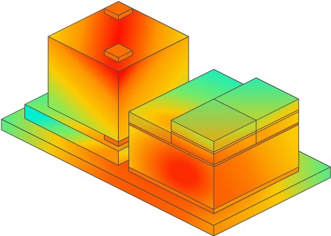
- Integrated thermal analysis: Calibre 3DThermal enables hierarchy-aware mapping from RTL through implementation and materials mapping to capture the effects of die thinning, underfill, etc. Design engineers can iteratively explore thermal gradients and adjust floorplans, block placements, or cooling solutions, optimizing long-term reliability.
- Multi-scale stress analysis: Calibre 3DStress empowers designers to simulate die warpage, thermal expansion, and piezoresistive effects during early floor planning. Its full-chip and block-level visualizations reveal potential hotspot locations, so designers can proactively address mechanical reliability concerns.
- Unified EM/IR analysis for digital and analog: mPower is the first and only power integrity solution that can provide signoff for electromigration, IR drop, and power integrity for analog and digital designs at scale. It automates current density extraction across 3D pathways, interposers, TSVs and redistribution layers. With mPower’s visualization tools, design engineers can immediately relate EM/IR risk back to physical design and reliability across operating conditions.
Siemens complete suite of 3D IC design and verification tools—including Innovator3D IC, the Aprisa digital implementation system, and Xpedition for PCB systems—works in harmony with advanced multiphysics simulators like Calibre 3DThermal and Calibre 3DStress solutions. Together, these tools extend beyond the capabilities of siloed domain solvers, enabling deep, accurate, and early assessment of 3D multiphysics risks—saving time and reducing late-stage surprises.
Learn more in our latest technical paper, A comprehensive approach to 3D IC physical verification: DRC, LVS and beyond.
Build a 3D digital twin with multiphysics insights
Leveraging the industry’s most comprehensive digital twin, Siemens extends 3D IC multiphysics analysis throughout the entire product lifecycle.
By maintaining an accurate digital representation from the transistor to the system levels, engineers can run predictive simulation and optimization, accounting for interactions down to the package, board, or even system levels. This continuous transfer of multiphysics results across levels of abstraction allows teams to validate whether a chiplet will behave as expected under real-world operating conditions.

In 3D IC architecture, electrical models alone are no longer sufficient. Chiplet electrical models must be augmented by multiphysics data captured from stack-level simulations. Back-annotating temperature and stress outcomes from package-level analysis into chiplet netlists provides the foundation for more accurate system-level electrical simulations. This closed-loop process is rapidly becoming essential for 3D IC signoff, ensuring that each chiplet operates within its intended performance and reliability envelope once assembled into a complete system.
Shift-left: Enable predictive multiphysics analysis
Waiting until signoff to evaluate thermal or mechanical risks can force late-stage redesigns—often when fixes are most costly and time-consuming. Siemens’ shift-left approach avoids this by introducing multiphysics simulations at the earliest stages of 3D IC planning, well before floorplanning and placement are locked in. Early assessments let engineers experiment with different chiplet placements, explore power delivery tradeoffs, and uncover potential thermal hotspots or stress concentrations long before committing to detailed implementation.
As a design evolves, designers can add more details: update placement, refine materials, and input realistic power estimates. Siemens solutions help streamline this evolution—supporting both guided automation and expert-driven control—so engineers can iterate efficiently without rebuilding the model at every stage.
Take a closer look: A modern multiphysics solver flow
Siemens’ multiphysics workflow is integrated with the Innovator3D IC™ Integrator. Innovator3D IC Integrator is a heterogeneous-integration cockpit that enables true STCO by constructing a unified, system-level digital twin—spanning dies, chiplets, interposers, and package. It preserves a single source of connectivity and intent across the full Calibre 3D IC verification and multiphysics tools. Once the system floorplan is defined in Innovater3D IC Integrator, it flows seamlessly into Calibre 3DSTACK, Calibre 3DThermal, Calibre 3DStress, and other analysis engines, eliminating redundant data recreation while ensuring consistent results from planning through signoff.
With this integration, our multiphysics workflow extends seamlessly from chiplet floorplanning and implementation through physical and electrical verification—ultimately ensuring timing integrity, thermal reliability, and system-level electrical performance. This unified environment enables true shift-left analysis, allowing teams to capture thermal and mechanical impacts early, guide or automate thermally and stress-aware placement decisions, and propagate those results upward for board and system level evaluations.
Here’s a typical IC verification and analysis flow:
- 3D floorplanning and connectivity: Start with Innovator3D IC Integrator to define block placements, interconnects, and initial power data.
- Physical verification: Run Calibre 3DSTACK for physical and circuit verification across the stack.
- Multiphysics analysis: Includes initial power and thermal analysis to flag major risks. The analysis tool gives feedback on optimizing for thermal placement, stress minimization, and signal integrity.
- Pull in the impacts of thermal-mechanical stress.
- Iterative closure to refine timing and electrical results.
By the time you reach signoff, most of the critical issues — thermal hotspots, stress concentrations, and parasitic interactions — have already been addressed. The results: DRC, LVS, and timing signoff become far more predictable, far less stressful, and significantly more robust for 3D IC designs.
If you’re ready to explore Siemens’ multiphysics flows for 3D IC design, please explore the resources available on our 3D IC design solutions page.