ESD verification in 3D ICs: Navigating unseen risks and new realities
By Dina Medhat
As a verification engineer facing a cutting-edge 3D IC design, a few immediate concerns might keep you up at night. The reputation of your product—and your peace of mind—depends on understanding and mitigating these ESD protection risks. What should you worry about? Whether your automated ESD verification tool can untangle complex connectivity, distinguish IO exposure, manage heterogenous integration, area and routing constraints and have visibility into “hidden” ESD risks.
The good news is that a strong pre-tapeout ESD protection verification solutions for 3D IC, like Calibre 3DPERC, overcome the limitations of traditional EDS verification for planar designs.
Why 3D ICs amplify ESD risks
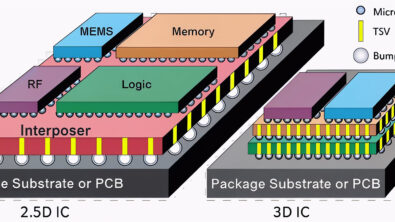
The move to 3D integration and advanced packaging has created boundless opportunity, but also introduced new challenges in IC reliability. Some corporate studies estimate that ESD-related losses can be as much as 10% of annual revenues for traditional designs. For 3D ICs, where more interfaces and advanced nodes magnify both the risk and complexity, the true financial impact could be even higher—and less predictable.
Several converging trends have transformed ESD protection from a well-understood checklist item to a potential design minefield:
- Increased sensitivity: As technology nodes shrink, devices become more susceptible to ESD damage. What was once a minor upset can now be catastrophic, especially in smaller geometries.
- Complex interfaces: 3D ICs commonly feature thousands of die-to-die connections, sometimes with ultra-fine bump pitches. Each interface is a new potential entry point for ESD, and they require novel approaches for effective protection.
- Design constraints: Traditional ESD clamps and protection schemes consume valuable die area. For advanced 3D stacks, where interconnect density is high, this is often impractical, demanding innovative solutions and stricter manufacturing controls.
- Hidden costs: The immediate consequences of ESD are rarely the full story. Down the line, unprotected or mis-verified paths can drive up costs through rework, late-stage testing, warranty claims, field service, and dissatisfied customers. Each step later in the process can multiply these costs exponentially.
In practice, verification engineers know that a defect missed in ESD verification rarely stays hidden. Instead, it can mushroom into expensive and disruptive failures—in manufacturing, in the supply chain, or in the hands of customers.
Learn how Marvell overcame ESD verification challenges for 3D IC designs by watching this video
Outgrowing traditional 3D IC ESD verification methods
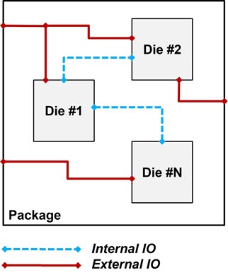
Historically, the recipe was simple: treat every I/O as exposed, apply full ESD protection, and check compliance. For 3D ICs, the situation exceeds the scope of those checklists. Now, not every I/O faces external threats; many connect only internally between stacked dies, and don’t need costly, large protection circuits (figure 2). Overprotection can lead to wasted area, unnecessary complexity, and higher power consumption, while under-protection leaves products exposed to major ESD events.
The cross-die connectivity in 3D ICs adds another layer of challenge. ESD clamps might reside on one die but serve several; design and verification now operate across technology domains, process nodes, and sometimes multiple foundry rules. Tracking ESD paths manually in a multi-die assembly is not just tedious—it’s a recipe for missed vulnerabilities.
Better 3D IC ESD verification through automation
To keep up, teams are moving from manual rule checks to smarter, assembly-level ESD verification. Modern solutions like Calibre 3DPERC recognize the need to automate:
- Comprehensive connection mapping—analyzing not just individual dies, but the netlist of the entire 3D assembly, including interposers and package-level interfaces.
- Automated IO classification—distinguishing between externally exposed and strictly internal IOs, ensuring the right level of ESD protection is applied to each.
- Cross-die analysis—identifying and reporting ESD risks that cross process or foundry boundaries.
- Optimization and reporting—presenting reliable identification of over- and under-protected nets, guiding teams toward the most area- and cost-efficient solutions.
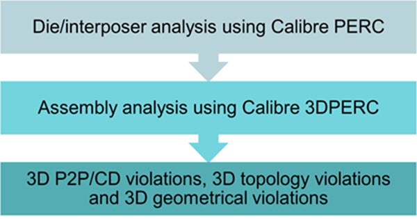
With this system-level approach (figure 3), the traditional anxiety around ESD verification can be replaced with real confidence—even as 3D assembly complexity continues to climb.
Navigating the new path for 3D IC ESD verification
3D ICs represent the future of high-performance electronics, but robust ESD verification is critical to realizing their potential. Data from across the industry is unambiguous: poor ESD management drains revenue, delays products, and erodes customer trust.
If you’re a verification engineer, design manager, or ESD specialist, ask yourself these questions:
- Are our ESD protection strategies matched to the complexity and sensitivity of our 3D IC designs?
- Can we reliably distinguish and protect only those interfaces that truly see external ESD risk?
- Are we leveraging tools that automate system-level analysis and reporting, rather than relying on incomplete manual checks?
- Do we understand the full downstream costs—beyond initial yield loss—associated with ESD failures?
Those questions will help you adopt solutions that transform ESD protection from a source of anxiety into a managed, auditable process—even as IC architectures get ever more complex. Staying ahead in this environment demands new thinking, system-aware strategies, and automation built for the realities of advanced packaging. The engineers who update their approach won’t just catch more bugs—they’ll protect their company’s bottom line and their reputation in the market.
Calibre 3DPERC supports robust ESD protection through these features:
- Verification tools that operate at the assembly level, not just per-die
- Automated IO classification tied directly to realistic physical connections and package interfaces
- Clear, actionable reports tracking every ESD protection path, across every die and technology
- Robust processes for handling design updates and team collaboration
Is your ESD verification strategy ready for the complexity of 3D ICs? If not, there’s never been a better time to explore advanced solutions like Calibre 3DPERC and learn how automation and best practices can radically reduce risk.
Read the new technical paper: Calibre 3DPERC: Your key to robust ESD solutions for 3D ICs


