Driving 3D IC innovation with Calibre multiphysics: A holistic approach for next-generation design
By John Ferguson
Fun fact: The concept of 3D integrated circuits (3D ICs) has been around since shortly after the first MOS IC was proposed in 1960. And in 1983, Fujitsu demonstrated the first 3D IC using through-silicon via (TSV) technology when they fabricated a 3D CMOS using laser beam recrystallization in. Fast-forward to today, and chip design and manufacturing has finally caught up to the demands and 3D ICs are transforming everything from AI accelerators to mobile devices. But this leap in complexity brings new challenges—including thermomechanical stress and reliability.
Most 3D IC design engineers are all familiar with the usual design headaches: stress, parasitics and timing closure. However, nothing throws a wrench into a 3D IC project quite like thermal effects. In 3D structures, heat has a much harder time escaping than in traditional 2D layouts. If thermal issues go unaddressed, they can spiral into electromigration, signal integrity degradation, timing failures, or even mechanical warpage.
So, how do we get ahead of these problems? Let’s talk about the value of a true multiphysics approach and how Siemens EDA is enabling design teams to collaborate—early and often—for successful 3D IC deployment.
3D IC multiphysics demands a holistic mindset
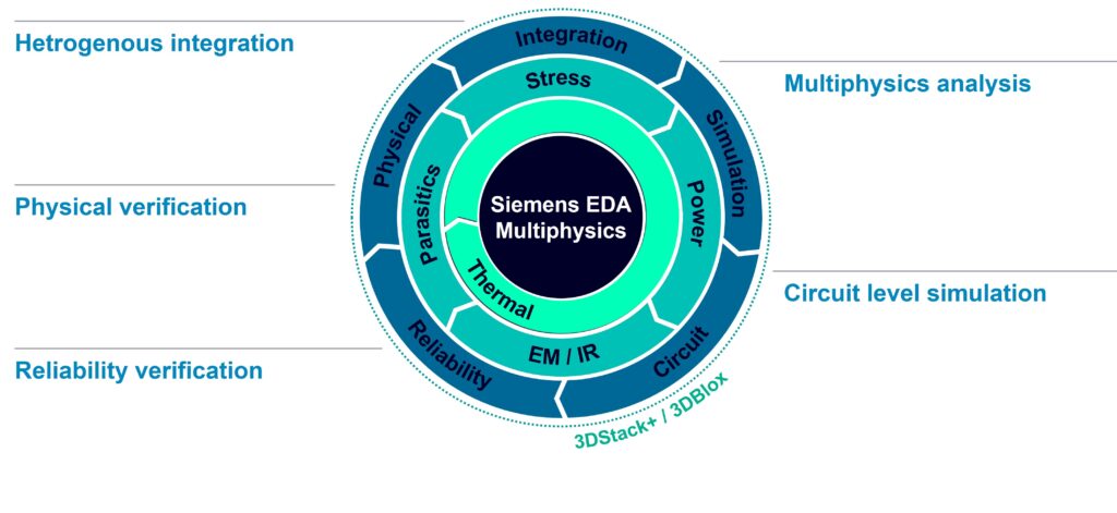
Siemens has been working closely with TSMC and other key eco-system partners to develop a holistic approach that enables the entire 3D IC workflow from design and verification through tape-out and manufacturing.
At Siemens, we see the move to 3D ICs as more than just a technological shift; it’s a shift in how the entire design, verification and manufacturing ecosystem works together. That’s why we work closely with partners like TSMC and other industry leaders to support a complete 3D IC workflow, from concept through verification and into manufacturing.
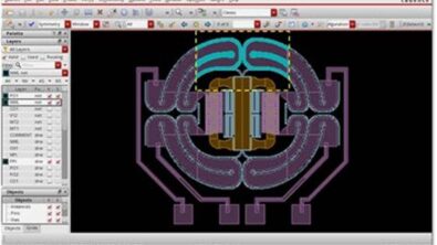
Our Calibre 3DSTACK platform brings physical and circuit verification together for heterogeneous 3D ICs, When combined with Calibre xACT for cross-die coupling extraction and our open integration philosophy, this approach offers both flexibility and robust customization. It allows customers to tackle both the generic and unique demands of each complex project.
And our complete suite of 3D IC design and verification tools—including Innovator3D IC, the Aprisa digital implementation system and Xpedition for PCB systems—works in harmony with advanced multiphysics simulators like Calibre 3DThermal and the latest Calibre 3DStress solutions.
Why does multiphysics matter in 3D IC design?

But first, what is meant by multiphysics? You have probably heard this one before: an object at rest stays at rest, unless acted on by an outside force. Conversely, an object in motion stays in motion unless acted on by an outside force. That’s Sir Isaac Newton’s Law of Entropy.
What we typically forget is the “outside force” bit, but in reality, that is the most important aspect. There are all sorts of forces impacting us every day: gravity, friction, solar, electric charges, thermal, mechanical stresses, sound, wind, rain and other weather disturbances, etc. And each one has the potential to impact others. For example, a sudden and significant change in temperature can result in air pressure change, precipitation, wind, static electricity, etc. We try hard to isolate some of these forces when possible, but the truth is it is never entirely possible. In other words, all physics is multiphysics!
In a 3D IC stack, the different physical phenomena—thermal, electrical and mechanical—all interact and become even more pronounced. Think about it like this: when you deliver power through stacked chiplets, the resulting current flow generates heat. This heat doesn’t just affect your transistors; it alters the behavior of your wires, impacts on-chip timing and can drive electromigration. But it doesn’t stop there. The different materials in the stack expand at varying rates when heated, creating mechanical stress and potentially causing warpage. In sensitive analog circuits, even small stress-induced distortions can affect performance.
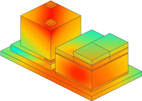
The bottom line? Every meaningful 3D IC analysis must account for these coupled behaviors. Calibre multiphysics solvers allow iterative, automated loops across power, thermal, stress and electrical domains—so you can reach true signoff with confidence.
Why shift left? Multiphysics analysis early in the design cycle?
If you only check for thermal or stress issues at signoff, you risk discovering problems when it’s already too late (and expensive) to make changes. That’s why we’ve embraced a “shift left” approach: run early multiphysics simulations during the 3D IC concept phase, before floorplanning or placement is finalized.
Early assessments let you experiment with different chiplet placements, explore power delivery tradeoffs and identify potential hotspots and stress points—before investing in detailed design.
As your design evolves, you can just add more detail: update placement, refine materials and input realistic power estimates. Our Calibre multiphysics tools are designed to automate as much of this process as possible. Whether you prefer hands-on control or a guided, automated flow, you’ll benefit from iterative simulation without starting from scratch at each stage.
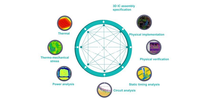
What does a modern multiphysics solver flow look like?
Growing from the Innovator 3D IC platform for chiplet floorplanning, placement and connectivity through to physical and electrical verification and Multiphysics analysis ultimately ensuring adequate timing and electrical integrity. It provides the ability to shift-left to capture impacts early in the design phase to help guide or automate thermally and stress aware chip placement optimization while also capturing the thermal impacts for further use at the board and even final product system level analysis.
Here’s a typical IC verification and analysis flow:
- 3D floorplanning and connectivity: You would start with Innovator 3DIC or integrate with your preferred chiplet planning tool. Define block placements, interconnects and initial power data.
- Physical verification: Run Calibre 3DSTACK for physical and circuit verification across the stack.
- Multiphysics analysis: This includes initial power and thermal analysis to flag major risks. The analysis tool gives feedback on optimizing for thermal placement, stress minimization and signal integrity
- Pull in the impacts of thermos-mechanical stress
- Iterative closure to refine timing and electrical results
By the time you reach signoff, you’ll have already addressed the big challenges—thermal hotspots, stress concentrations and parasitic impacts—making your DRC, LVS and timing checks far less stressful.
Want to go deeper?
If you’re ready to explore Siemens multiphysics flows for 3D IC design, explore the resources available on our 3D IC design solutions page.
3D ICs may have a long history, but modern multiphysics design is the key to making them reliable, scalable and ready for the future. Let’s drive innovation together.