Silicon Photonics Verification: A Light in the Tunnel
By Omar El-Sewefy – Mentor, A Siemens Business
Do silicon photonics designs need new verification tools? Turns out, expanding established electronic IC verification functionality will work just fine.
The silicon photonics market is growing rapidly. As production ramps up, designers are recognizing the need for a stable, automated design verification strategy, similar to what electronic ICs enjoy today. The first challenge for EDA companies is to find ways to handle silicon photonics’ geometrical construction, which typically includes a wide variety of curvilinear structures. Unlike the Manhattan components of electronic ICs, with their neat right angles and straight lines, silicon photonics elements wave and curve and bend in all directions. The second challenge is the lack of a traditional circuit schematic. Without one, designers struggle to ensure photonics circuit ports are properly connected, and to accurately recognize all devices and device parameters. And lastly, predicting manufacturing results to understand and improve circuit behavior is crucial to meeting performance specifications and market expectations.
But never fear…EDA has come through once again. In fact, it turns out that we can achieve the required degree of accuracy with only minor changes to existing electronic IC verification toolsets. For example, equation-based DRC uses flexible mathematical expressions to provide a customizable physical modeling capability that enables designers to evaluate and optimize a wide range of physical conditions in electronic ICs. Turns out, that same flexibility can be put to use to more accurately measure elements found in photonics ICs, such as bend curvature and curvilinear path.
In photonics circuit verification, the lack of a SPICE source list has similarly been overcome. Where electronic layout vs. schematic (LVS) would extract the assumed curvature and match it to a source, shape-matching LVS, a new method of validating curvilinear design, starts with the source and validates curvature.
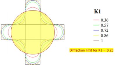
Then there’s the issue of manufacturing simulation. The final shapes of photonics circuits have a direct impact of circuit performance, so understanding the impact of lithography on the final product is crucial. Until recently, designers have typically relied on multiple iterations of physical device manufacturing, which is both time-consuming and extremely expensive. Now, however, photonics designers can obtain litho-friendly process design kits from the foundry and use litho-friendly design software to run process simulation checks and modify their designs to meet manufacturability and performance targets.
Silicon photonics is a fascinating concept that is rapidly becoming a reality in today’s electronics. To learn more about the techniques and tools being used in silicon photonics verification, read my white paper, Physical verification for silicon photonics: challenges and solutions.


