2017 Will Be B-I-G
By Michael White – Mentor, A Siemens Business
Trends, plans, and advice on what you can do to succeed.
It was an unusually cold, snowy, and rainy January and February here in the Pacific Northwest, which means our spring was a little later than usual. Despite that, when looking out my window through the rain back then, I still saw the first crocus and tulip bulbs starting to push up through the soil and bloom. Growth is a fine theme when looking at 2017, because we are going to see it in many places.
10 nm hits it B-I-G in 2017
Test chips dominated 2016, with a handful of early 10-nm production designs. 2017 is the year of volume manufacturing for 10 nm, and when I say volume, I mean VOLUME. Many of the early 10-nm designs are targeted at consumer (and, more specifically, mobile) applications showing up in this year’s most interesting products. Press releases have emerged from, among many, Samsung on its introduction of the first mass-produced system-on-chip (SoC) using 10 nm, Samsung and Qualcomm using 10 nm for its latest Snapdragon 835 mobile processor, Mediatek’s Helio X30 processor, and LG’s next-generation processor—all on 10-nm processes.
While Intel has been shipping its most advanced microprocessors using 14-nm technology for a while, at this year’s Consumer Electronics Show, Intel CEO Brian Krzanich took to the stage with a prototype 2-in-1 machine he promised was running a 10-nm Cannonlake CPU. So, regardless of where you might fall on the argument of Intel vs. TSMC, etc., over the marketing labeling of “10 nm,” they are building 10-nm products.
Of course, any discussion on advanced technology must also include the “fruit” company. The blogosphere has been awash with discussion about the next-generation iPhone 8 moving to 10 nm for a range of its components, including the A11 Fusion application processor. The industry won’t see an official confirmation of this until the iPhone 8 is actually released, but all bets are on its use of 10 nm.
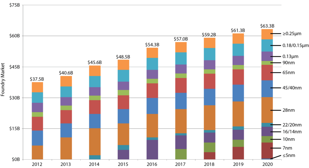
When 10 nm does come this year, it will come like an avalanche. As you can see in the figure, 10 nm didn’t even register in any material way in 2016. In 2017, it leaps from $0B to $5.0B. This is analogous to what the industry demonstrated in the jump from 20 nm to 16/14 nm rolling into 2015.
One might ask “How is it possible to ramp to nearly 10% of industry-wide revenue in a single year (9.9% for 16/14 nm and 9.0% est. for 10 nm)?” The answer is twofold. First, multiple foundry ecosystems are making the jump in the same year (e.g., TSMC and Samsung in 2015, and TSMC, Samsung, and Intel Custom Foundry in 2017). Secondly, by design, the foundries are leveraging the prior node process technology and wafer-manufacturing equipment to the largest extent possible. By doing so, they minimize the process development and maturation effort to the largest extent possible—reducing the cost and time required to ramp to volume production yields. Also, by maintaining as much node-over-node consistency as possible, they can minimize the cost and schedule of having to build completely new wafer-fabrication operations for each new node introduction.
What TSMC said in its 2016 Open Innovation Platform and Technology Forum events (and reiterated in 2017) is that it has been able to maintain on the order of 90% process equipment commonality between 20 nm and 16 nm, from 16 nm to 10 nm this year, and 10 nm to 7 nm over next year. We in the design community must react to certain material design rule and intellectual-property (IP) changes, but the process foundation we are building on is more stable and ramps faster compared to what we experienced years ago. The drama and delays in the 65 nm to 45/40 nm and 32/28 nm to 20 nm FinFET jumps come to mind…
In 2016, we saw the initial wave of 10-nm production designs being released into risk production, and now, in 2017, we see those designs and others are rolling into volume production. Advanced mobile (e.g., cell phones, etc.) and high-performance computing for Big Data and data centers will be the major drivers.
1. The chart shows the evolution of the foundry market by feature dimension.1 (Source: International Business Strategies Inc.)
7-nm Starts
It’s become evident that 7 nm is an entirely different type of node compared to the past, with lithography approaches and timing all over the map. Previously, everyone introduced a new node using more or less the same 365 nm, 248 nm, 193 nm, and 193i scanners on more or less the same timing. With 7 nm, not so much…
At its Executive Forum, Samsung clearly stated that the company’s 7-nm plan is extreme ultraviolet (EUV) lithography. Others (TSMC, GLOBALFOUNDRIES, etc.) are coming to market earlier with 193i scanners and an ever-growing plethora of multi-patterning (MP) strategies, including double patterning (DP), triple patterning (TP), quadruple patterning (QP), and spacer-assisted double patterning (SADP)—and /or combinations of all of them!
Even though no two foundries’ approach to DP, TP, QP or SADP is the same, they’re all pursuing a strategy of minimizing change as well as the number of exposures/masks. The specific mix of DP, TP, QP, and SADP (and potentially EUV) will vary by foundry. However, you will be designing with some form of multi-patterning beyond basic DP for those layers where there’s no other way to obtain the required feature size and pitch without adding additional exposure steps. In its current state of maturity, EUV, like MP over the last several nodes, will be used on a limited number of layers, if you see it at all. I project the EUV market introduction will be gradual across more than one node. More on this in some future article.
Development of the 7-nm process has been underway for several years now. Early IP development for 7 nm began last year within the leading fabless companies and third-party IP providers. 2017 brings more of the same, with some of the leading foundry ecosystems moving into test chips and risk production. Analogous to the discussion above on the next node jumps, expect to see a jump in revenue next year as leaders move to 7 nm.
Process Offerings Proliferate
I find it funny how things change over time. When I talked with foundries contemplating the 28-nm to 20-nm jump, in contrast to every node before, they all talked of having a single 20-nm process offering. Just one. Look around the industry now and you will see a range of offerings at each node for each foundry ecosystem. The other thing we will see more of this year is the introduction of new offerings for the most popular processes. Samsung announced its 10LPU (10 nm variant) for reduced area. And TSMC will be rolling out the new N12 (N16FF+ variant) for reduced die size and lower-power requirements.
We also continue to see more process offerings introduced for reduced power in general sensors, image sensors, application processors, etc., targeting mobile/remote Internet of Things (IoT) applications. During 2016, several new offerings from TSMC were ≥ 28-nm ultra-low power, and you shouldn’t be surprised to see more in 2017. GLOBALFOUNDRIES is rolling out its lower-power IoT-focused 22FDX and 12FDX offerings. The established nodes ≥ 28 nm are anything but static. Expect more derivative processes off the initial node offering coming soon to a fab near you!
Summary
No doubt, 2017 should continue to be a very interesting year, regardless of the technology node your products are targeting. We will see a step function growth in the number of wafer starts (and revenue) for 10-nm designs. Early adopters at 7 nm are already starting to create IP and will be taping out early test chip designs. For those pursuing IoT and connectivity-related applications, there will be continued evolution of 0.18-µm, 130-nm, 65-nm, 45/40-nm, and 28-nm processes, design kits, and design rules to support the more complex and ultra-low power designs the market now demands.
One thing is certain: With all of this change, staying aligned and in sync with your foundry has never been more critical to ensure smooth design tapeouts. Using the same electronic-design-automation (EDA) tools that your foundry employs for its internal process development and design verification helps ensure you’ll reach tapeout as quickly as possible—creating critical market advantage. 2017 will be a year of change and growth for whatever node you’re targeting for your next design. Anticipation and preparation will be your keys to success.
Reference
1. International Business Strategies Inc. (2016). Foundry Market Trends and Strategic Implications (Global Semiconductor Industry Service Report). Los Gatos, CA. www.ibs-inc.net
This article was originally published on www.electronicdesign.com


