Towards robust optimal sensor placement for thermal digital twins in electronics
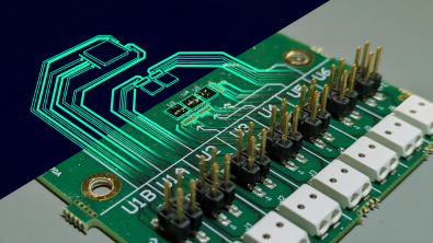
Thermal Digital Twins to monitor electronics reliability
How do you know how hot something is when you can’t actually put a temperature sensor there? That question sits at the heart of the collaboration between Siemens and imec, introduced in the last blogpost, as part of the EU-funded Marie Skłodowska-Curie project MIRELAI to develop physics-based Digital Twins (DT) for electronics.
The goal is to estimate in-operation temperatures in critical and possibly inaccessible locations, relying on just a few sensors. After all, physical sensors represent a cost, take up valuable space and, inconveniently, can’t always be placed exactly where you most want to know the temperature.
Temperature is the major cause of electronic failure1 and, indeed, a key parameter in assessing electronics reliability. Put simply, if we want to understand how reliable an electronic system will be, we need to know how hot its critical parts get. The reason lies in the different materials and complexities adopted in such systems. Materials expand and contract differently with temperature, causing internal stresses that ultimately lead to fracture of electrical connections or other kinds of failure.
So how can a Digital Twin fill in the temperature information that the physical sensors can’t provide? This is where the Augmented Kalman Filter (AKF) comes in. It uses real-time measurements and updates the employed model with estimates of unknown (or uncertain) system parameters so that it reflects the real system temperatures. With Simcenter Flotherm, a high-fidelity model is built using the Finite Volume Method, and a Reduced Order Model is exported for real-time execution. High-fidelity physics, in other words, but distilled into something fast enough to keep pace with the real system.
Where to put sensors
Having established that we don’t want sensors everywhere, the obvious next question is: where should we put the ones we do have? Estimation performance relies on the locations of the sensors used in the DT. Optimal Sensor Placement (OSP)2 strategies have been developed to maximise estimation performance while minimising the number of sensors. The aim is simple enough: get the most useful thermal information from the fewest physical measurements. For example, sensors can be progressively removed from the DT, starting from an initial coarse pool of sensors and looking at an estimation performance metric of interest, i.e. the unknowns estimate covariance matrix, while removing sensors. This strategy selects the most informative sensor locations.
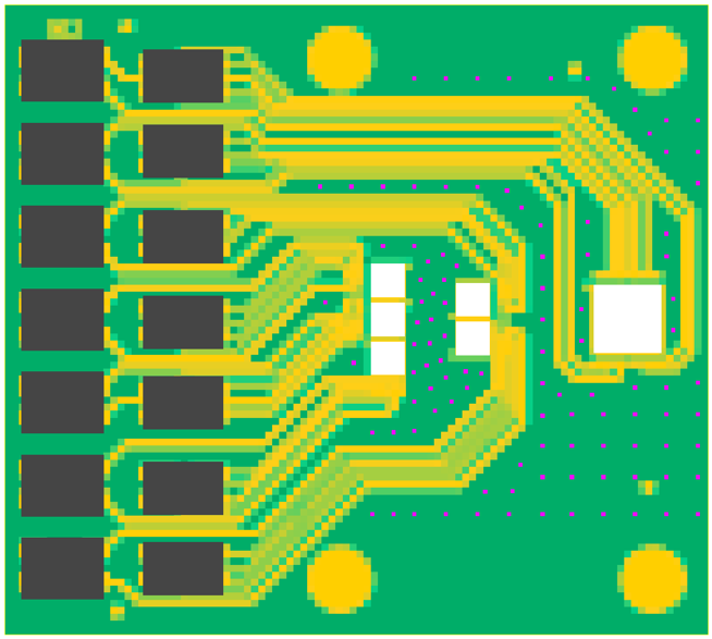
In a previous study3, we tested state-of-art OSP on the thermal model of the Printed Circuit Board Assembly (PCBA) in Fig. 1 featuring 5 chips of dimensions 3.2mmX3.2mm and a chip of dimensions 6.4mmX6.4mm. Temperature sensors on the top were assumed to be installed on top, in contact with the dielectric in order to avoid any kind of interference with circuitry. Here, however, we hit an interesting problem. The most informative sensor locations tended to be close to chips, where temperature varies sensitively, as in Fig. 2, due to the low thermal conductivity of FR4, a common dielectric material adopted for electronic boards. And therein lies the problem. In such cases, matching the sensor location in the model with the corresponding location in the real system is critical to avoid the introduction of measurement bias, which would translate into unreliable estimates.

So, can OSP itself be made more robust to this uncertainty? To tackle this issue, OSP was modified to include the temperature uncertainty in sensor locations depending on thermal gradients, i.e. temperature variation on the plane, and assuming a possible sensor location uncertainty. This uncertainty component worked as a weighting term for sensing locations and helped OSP identify more reliable sensing locations, resulting in more reliable thermal estimates. However, the developed approach consisted of modifying the AKF definition for the OSP algorithm execution, considering the measurement bias uncertainty as an aleatoric uncertainty, like in the case of measurement noise, instead of an epistemic uncertainty, which results in persistent error, i.e. actually a bias.
This leads naturally to the next question: can we do better? The next step is represented by the definition of a new metric to be used in the OSP4, to achieve a more robust sensor placement without considering the measurement bias as an aleatoric uncertainty in the AKF definition. The metric is obtained by noticing that the estimated parameters in the AKF can be split into three different components:
- a signal component due to the actual parameter value,
- a noise component due to the measurement noise,
- a bias component due to measurement bias.
At steady-state, the AKF is known to converge to the parameter value; the remainder uncertainty is due to measurement noise and bias. The new metric adopted in OSP, therefore, considers these two components separately, while preserving the AKF definition, at steady-state.these two components separately, while preserving the AKF definition, at steady-state.
Impact of the new metric on OSP
Enough theory then, what happens when we actually try it? The proposed methodology has been tested on the PCBA model in Fig. 1, assuming it lies on an aluminium plate. The model is truncated at the bottom of the board, where a boundary condition with a high (but impossible to measure) Heat Transfer Coefficient (HTC) models the thermal resistance at the contact. We assumed that, together with the bottom HTC, the power dissipation of the 6 chips is unknown as well, that sensors can be located only on top of the board, and that temperature measurements from the chips are not available.
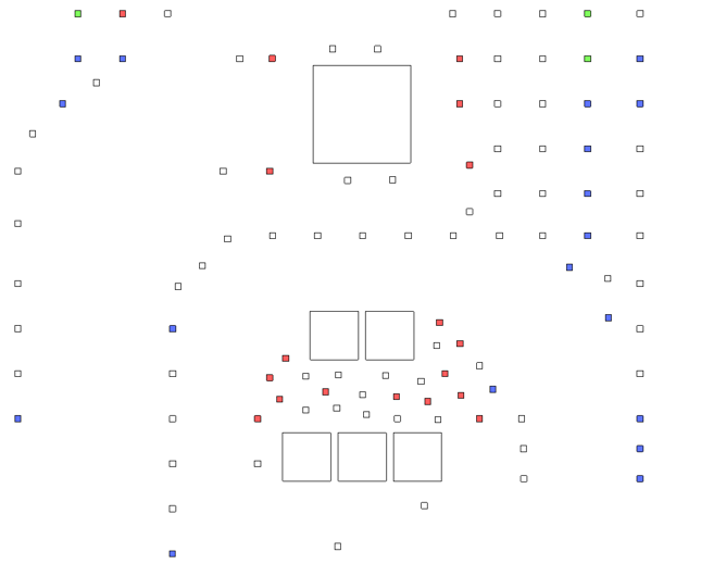
With the considered setup, the OSP strategies from the previous and new studies were executed and compared. The two approaches selected slightly different sensor configurations. So far, perhaps not especially surprising. What is more interesting is where they started removing sensors. The new approach started from the center of the board and lowered the estimation bias uncertainty, as reported in Fig. 3. This is different from the other approach that tackled locations at the borders first. This methodology therefore highlights and tackles the problem of redundancy of correlated measurements in estimation problems when affected by measurement bias.
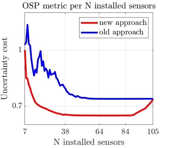
Does that mean the problem is solved? Not quite. The final uncertainty given by two different optimal sensor configurations, with 7 sensors, is similar, highlighting the challenge represented by estimating temperatures of a PCBA when installing temperature sensors on FR4 on top of the board.
In conclusion
Digital Twins enable temperature estimation in electronic devices in inaccessible locations with a limited number of sensors. In effect, a handful of physical sensors can provide the measurements needed to support many more virtual sensors throughout the system. The choice of sensor locations, though, can critically impact estimation reliability. Optimal Sensor Placement can be informed of thermal gradients and assumed sensor location uncertainty to return more reliable sensing locations. In particular, the new approach highlights and deals with the problem of conflicting measurements when affected by uncertain bias. However, the resulting estimation uncertainty with optimal sensor configurations is similar for both approaches, indicating the challenge of temperature estimation of a PCBA when installing temperature sensors in contact with FR4.
On Monday September 7, 2026 at the 32nd edition of the ISMA Conference on Noise and Vibration Engineering in Leuven (Belgium), Matteo Depaola presents our paper4
on robust optimal sensor placement for thermal virtual sensing in electronic systems at 14:15 CEST. Please refer to the ISMA conference website for more information.
Acknowledgements
The European Commission is gratefully acknowledged for funding the Horizon Europe research and innovation programme, which includes the support for the Marie Skłodowska-Curie Action (MSCA), including the Industrial Doctoral Network MIRELAI (MIcroelectronics RELiability driven by Artificial Intelligence) with Grant agreement ID 101072491.
MIRELAI has the ambition to address the challenges of reliability, sustainability, and verification efforts related to the production of microelectronics components, and boost Europe’s innovation capacity and competitiveness in the market. To achieve this goal, the project recruited 13 doctoral candidates (DCs) to investigate the physics of degradation and reduce testing and verification efforts across the value chain of electronic components and systems, while providing invaluable skills to the next generation of engineers.
References
- H. C. Fortna, “Avionics integrity issues presented during naecon (national aerospace and electronics convention) 1984,” 1984. ↩︎
- R. Cumbo, L. Mazzanti, T. Tamarozzi, P. Jiranek, W. Desmet and F. Naets, “Advanced optimal sensor placement for kalman-based multiple-input estimation,” Mechanical Systems and Signal Processing, vol. 160, 2021. ↩︎
- M. Depaola, D. De Gregoriis, R. Bornoff, B. Vandevelde and D. Moens, “Optimal Sensor Placement for Thermal Virtual Sensing in Electronic Systems Using Augmented Kalman Filtering,” in 31st International Workshop on Thermal Investigations of ICs and Systems (THERMINIC), Naples, 2025. ↩︎
- M. Depaola, D. De Gregoriis, R. Bornoff, B. Vandevelde and D. Moens, “Robust optimal sensor placement for thermal virtual sensing in electronic systems,” Proceedings of ISMA/USD 2026, 2026. ↩︎