Reduce Advanced-Node Risk with an Integrated FinFET Layout Flow

We Have a New L-Edit/FinFET Training for You!
As semiconductor technologies continue scaling into advanced nodes, layout design has evolved from simple geometry drafting into a precision-driven engineering discipline. In FinFET technologies, success depends on strict grid alignment, quantified device construction, complex context-based spacing rules, and immediate verification feedback. Design environments that fail to support these constraints natively create unnecessary risk, iteration cycles, and costly delays. By combining L-Edit with Calibre RealTime, you can establish a streamlined, verification-aware layout flow built specifically for advanced node challenges.
Unlike planar CMOS, FinFET devices introduce width quantization defined by the number of fins, strict fin and poly pitch requirements, and routing constrained to predefined track grids. Even minor off-grid geometries can trigger DRC violations or patterning conflicts. For this reason, layout must begin with a disciplined grid configuration. Within L-Edit, you can define the fin pitch, poly pitch, and routing track grids directly in the layout environment, ensuring that all geometry snaps to technology-approved increments. This grid-driven methodology embeds correctness into the design process from the start.
Advanced nodes also introduce complex, context-dependent spacing rules. Instead of managing these rules manually, L-Edit enables Width-Spacing Pattern (WSP) definitions that encapsulate spacing behavior based on width and geometric conditions. WSP definitions can be grouped into WSP sets and applied to routing regions, ensuring that all geometry within those regions automatically follows the appropriate spacing logic. This approach significantly reduces spacing violations and improves layout consistency.
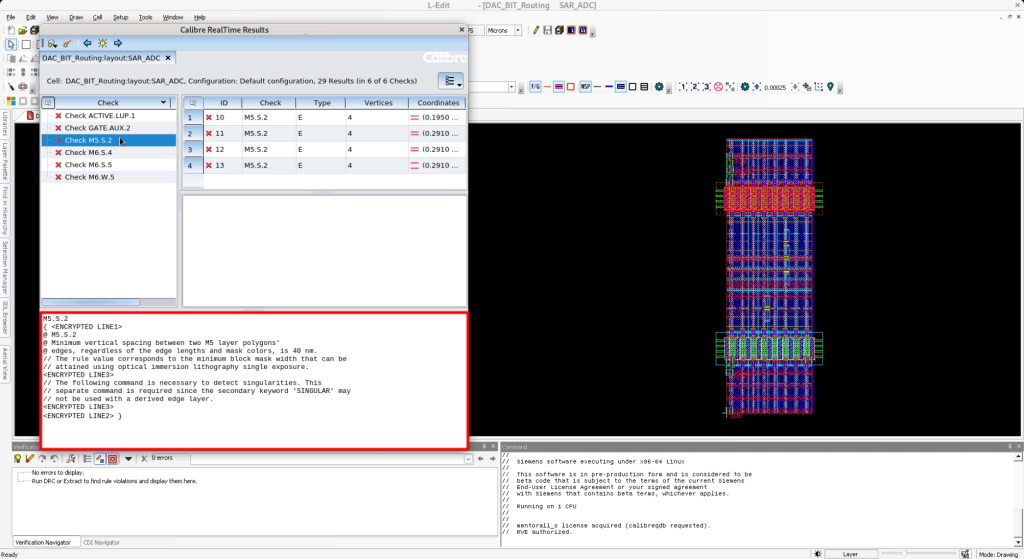
Verification remains the final and most critical stage of advanced node layout and waiting for batch DRC results is no longer efficient. Integrating Calibre RealTime directly within the L-Edit environment transforms verification into an interactive process. You can receive immediate feedback on rule violations, pattern-matching conflicts, and spacing inconsistencies as they occur.
In the era of FinFET technology, layout excellence is no longer optional; it is strategic. L-Edit provides the structured, grid-accurate design environment required to build FinFET layouts correctly from the start, while Calibre RealTime ensures those layouts meet advanced manufacturing constraints before signoff. Together, they create a powerful ecosystem that transforms advanced node layout from a high-risk challenge into a controlled, scalable engineering process.
Visit Siemens Xcelerator Academy and register for our upcoming “L-Edit Advanced Nodes for FinFET” classes at: Siemens Xcelerator Academy: Live Training Course Catalog
This training course is also available as Self-Paced Training, learn more at: Self-paced training | Siemens
At the end of your learning journey, you can test your knowledge and earn Siemens EDA Level1 certification badge!
Author: Yarah Keelany, Customer Training Engineer, Siemens EDA Learning Services