PCB Creepage

As I was teaching a class, I was asked a question about how to do notches for creepage. Well, that was new question for me, so I had to do a little bit of research. First, what was he actually talking about. In the PCB world, we are all familiar with the term clearance. It is the air distance between two objects, and it is a common control factor in placing and routing PCB designs. Creepage is different. It is the spacing rule that is applied between two conductive elements over an insulating surface – the substrate. It turns out that this can be a very important factor when dealing with high-voltage applications on a PCB design. Creepage will always be equal to or greater that the clearance between two conductive elements. There are some good discussions online about this topic – just search for “PCB Creepage”.
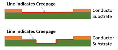
Many times in a high voltage environment, it becomes important to increase the creepage between two conductive elements. This can be done by adding notches in the substrate, thereby increasing the substrate surface area between the two elements by adding vertical elements to the substrate surface in addition to the horizontal elements.
The customer’s question was how to do this in Xpedition Layout. Just thinking off of the top of my head I came up with two ways.
The first is to just call it out in fabrication. Make a User defined layer called something like “Creepage Slots”, and then draw the slots as a rectangle draw object between the conductive elements. The fabricator would then have to be provided with the depth of the slot to include during fabrication. I would probably also include a routing obstruct around that object to prevent edits from pushing other objects, or even the objects that are being separated from the slots, into that area.
The second method would be available if the slot was to be cut completely through a single layer of the substrate, say from layer 1 to layer 2. In that case the slot could be defined as a drawn cavity, a cutout that goes between layers.
Creepage control through a notch in the substrate is an element in high-voltage applications on a PCB design. There may be other ways to provide the definition of that notch in Xpedition Layout.
For more details on the content of PCB Layout in Xpedition Flow, visit here.
Author: Larry Stones, Principal Instructional Designer, Siemens EDA Learning Services