Practical advice on PCB stackup planning
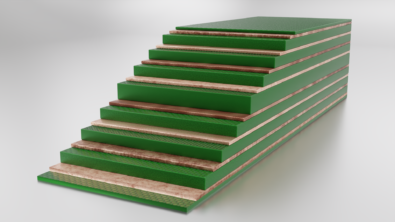
The more technology advances, the more attention we must pay to every aspect of printed circuit board (PCB) design, including construction. And with the trend line of circuit speeds accelerating exponentially, the subject of PCB stackups increasingly is coming into focus.
We often are guilty of deflecting or dismissing topics which someone else has handled for us in the past. However, with PCB stackups affecting our products’ costs, performance and availability, we can no longer pass the buck. As designers we must take ownership of the stackup decisions.
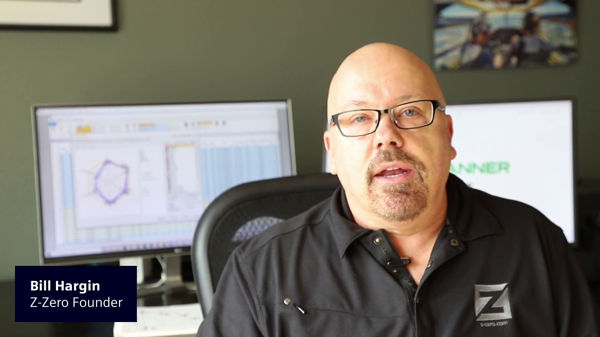
In a very short video, Bill Hargin, Founder of Z-zero provides perspective on the importance of PCB stackups in today’s designs. Bill offers his view on why stackup planning is important with a voice of deep industry experience. Simulate what you are going to build. It’s an obvious objective, but it takes a lot of experience to create straight forward solutions to complex problems.
He is authoritative and practical when he shares the significance of a correct PCB stackup on signal integrity simulation. And when you hear his comments on the challenges of working with multiple fabricators you’ll nod in agreement.
Give it a watch. It’s worth 7 minutes of your time.
