What’s new in Valor NPI v11.5
Valor NPI Introduction
Decisions made during PCB layout directly affect the success of your NPI process. Any problem found by your supply chain will cause a delay at minimum, or worse, costly scrap. And if designs are reviewed differently by the PCB fabrication or assembly supplier than by the designer using EDA tools, yield, cost, and reliability risks remain high. As a result, leading electronic design companies have found that “left-shifting” Valor NPI technology concurrently into their PCB design process saves expensive revision spins and improves the quality of the final product.
Valor NPI 11.5 continues to introduce new and exciting capabilities in MRA-Revolution, with a more complete Classification set which includes design preparations and analysis use of copper reference layers. Comparing an ODB++ to fabricator changes becomes easy and precise with the new CAM Compare flow and the first connection to stackup setup is established with Z-Planner integration.
Take an in-depth look into Valor NPI 11.5 new capabilities:
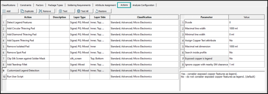
Consolidate your MRA-Revolution flow with the Analysis Definition Manager addition of design preparations
The Analysis Definition Manager new addition of DFM, cleanup and optimization actions allow a consolidated flow addressing design preparation steps as part of MRA Revolution.
The supported actions are Copper Balancing, NFP Removal, Teardrop Creation, Legend Detection, Silk Screen Optimization and User Script.
Analyze solder mask, solder paste and silk screen layers against their respective copper reference layers
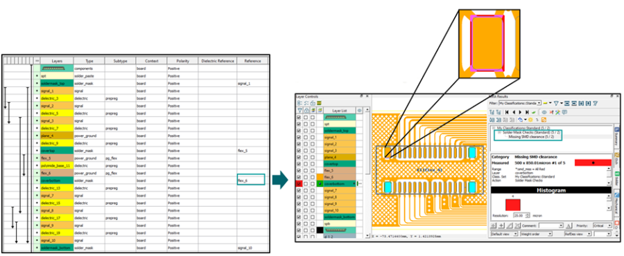
Rigid-flex or embedded component designs could have multiple solder mask, solder paste and silk screen layers to support the iterated manufacturing process. Each of those layers should be analyzed against its applicable copper layer to avoid missing violations or false alarms.
Improved drawn thermal recognition support during Drill and Power & Ground analyses
Drawn thermals of PTH pads on positive power & ground layers are identified and analyzed in Drill and Power & Ground checks.
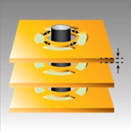
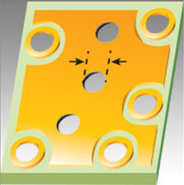
Large Pin Thermal Connection
Reports the cumulative area of thermals connecting the through pin to layers, for holes larger than the value of Analysis Configuration Parameter “Drill – minimum pin diameter” (default 80 mils/2032 microns).
Drills with mounting or tooling hole attributes are ignored.
Connection areas larger than the value specified are reported in sq.mil/mu.
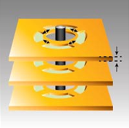
Small Pin Thermal Connection
Reports the cumulative area of thermals connecting the through pin to layers, for holes smaller than the value of Analysis Configuration Parameter “Drill – minimum pin diameter” (defaults 80 mils/2032 microns).
Drills with mounting or tooling hole attributes are ignored.
Connection areas larger than the value specified are reported in sq.mil/mu.
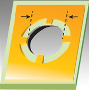
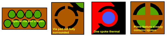
No Interceding Thermal Pad
Reports on positive layers PTH pins connected directly to a plane and without an interceding thermal pad which may result in the hole to not being properly fitted during the soldering wave process.
No Interceding Thermal
Reports PTH pins connected directly to a plane without a thermal which may result in the hole to not being properly filled during the soldering wave process.
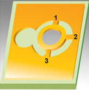
Thermal Spoke Count
On positive copper layers thermal connections are represented by line drawn connections. However, due to placement the connection may need to be relocated or eliminated completely. Positive Layer spoke Count contains the minimum number of required line spoke for each connector. A reduction too great may impact electrical performance or reliability.
Optimize comparison by managing etch compensation and drill resize changes
Gerber and drill data received back from the PCB Fabricator might include intentional enlargement of copper to compensate the etching process and the resizing of drill data to accommodate plating. The new CAM Compare functionality enables a user to compare the original ODB++ product model with data received while managing such changes and eliminating false alarms.
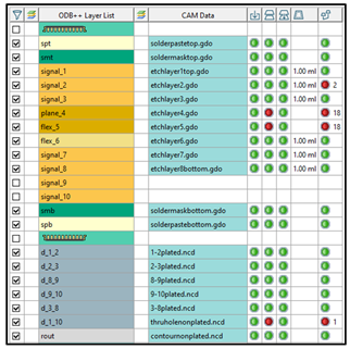
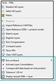
CAM Compare
The following options are added in the Tools menu and to CAM Compare toolbar:
- Run layers compare on board/Profile.
- Allow consolidation of CAM layers data into one layer.
- Compare drill data based on hole center position instead of size differences.
- After the compare tolerance directly from CAM Compare.
- Review compare results while displaying the source ODB++ layer data as resized to mitigate etch compensation changes.
- Calculated resize as identified based on the typical Pad resize is displayed for matched layers.
- Number of areas with differences is displayed in the compare results column.
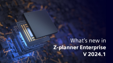
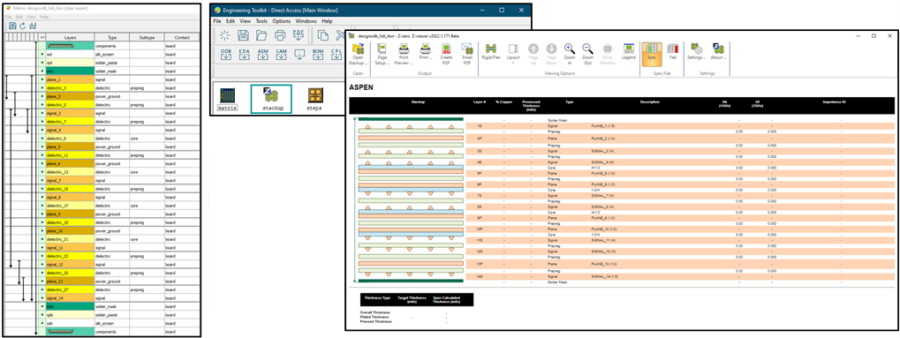
ODB++ Stackup review in Z-planner and Z-viewer directly from Valor NPI
Z-planner Enterprise is a field-solver based PCB stackup planning and materials selection software that provides complete control over not only the design of a stackup, but also the fabrication of the stackup. Valor NPI supports the review of the stackup when either the free Z-viewer or within Z-planner Enterprise is installed.
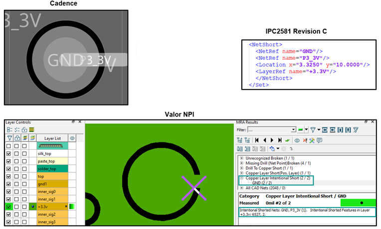
Support of intended shorts data from IPC2581 Revision C
NetShort information, required to identify intentional shorts in Netlist Analyzer, is read from IPC2581 Revision C files.