PCB Stackup Design e-book
Bill Hargin of Z-zero recently released an e-book: Stackups: The Design within the Design. The book explores the methodology and thought process that goes into planning a PCB stackup, exploring it within what he refers to as ‘the design within the design’. While there is a lot to this book – it is short, but densely packed with information – one of the initial take-aways struck me as brilliant and that takeaway exists within the title itself.
The design within the design
When we talk about PCB design we are using an older terminology, a term that fit perfectly a decade ago, but that has since evolved. Perhaps now is a good enough time to revisit it. What has historically been thought of as PCB design is just one step of the process; the layout. With many of the other aspects of the process being removed from the moniker of ‘design’. For stackup design, the time to change has come, and the time to think about your stackup as a design consideration is now.
A decade ago we hadn’t reached the point where Signal Integrity (SI) had to be carefully watched across the board. You could send your design to any Fabricator and just rely on them to produce your board. They would all use FR-4 and everything within your design would work out from a materials perspective.
Today, with the exponential increase in signal speed, we have more challenging loss budgets to meet, which necessitate higher overall SI. A company will make huge investments to resolve SI issue like skew, crosstalk, and power distribution problems after they have occurred. As with all DFM, the preferred solution comes earlier in workflow before these issues occur and inflate the cost of their solution. An early solution is a cheap solution.
Stackup planning determines SI success
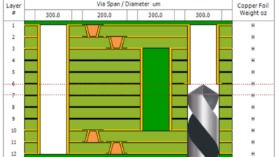
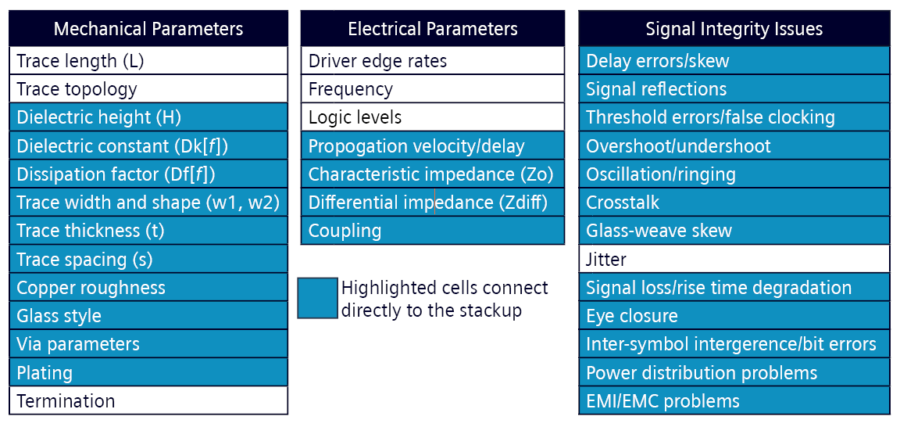
If we take a step back from our potential SI issues and examine some of the mechanical parameters of our boards, the majority of these can be linked to electrical parameters that then go on to produce signal integrity issues later in the build. If, for example, we want to minimize fall off from glass weave skew, this needs to be done in the stackup, likewise power distribution problems, crosstalk, skew, differential impedance, all lead directly back to decisions made in the stackup.
The stackup forms the core of your high speed design – it touches every part of your build, and the early design decision made here have huge ramifications later on in your design.
Controlling Signal Loss in the Stackup
So what are going to do about it? A tempting solution for this can be to just spend your way out of the problem – avoid design by intentionally overdesigning. If this is your company’s solution, and you produce at scale, then you are potentially leaving a lot of money on the table. If you are overdesigning while also pressuring your fabricators to reduce prices, then it is time to re-evaluation your situation. These are your technology partners, let’s work with your fabricators to reduce your costs, instead of relying on them to do it for you.
In Bill Hargin’s e-book, ‘Stackups: The Design within the Design,’ he notes; “In my experience, if you plan ahead and do careful loss planning, you can save over 10% on bare-board costs by working with a sharp pencil, having the right tools, and planning ahead.”
While not the final word on the subject of stackups, Bill’s e-book goes a long way to helping you plan ahead, providing an important voice in a space that is surprisingly lacking in content. I would also recommend exploring Z-planner Enterprise, a stackup tool that Bill has spent years developing. Now all you need is a sharp pencil.