Digitalizing PCB development processes for autonomous vehicles – part 3 of 8
The printed circuit board development process will play a major role in the safety and reliability of electronic systems in the design and development of autonomous and electric vehicles, including advanced driver assistance systems. All aspects of such systems need to be accounted for as well in the PCB development process. These aspects can include the operational environment, power duty cycles, component tolerances, assembly and manufacturing variance.
Moreover, costs and timing are critical. With unlimited budgets and time, it’s straightforward to develop such systems. But life is not so accommodating where time-to-market to beat the competition is a decisive ingredient for success.
An integrated PCB development process, which includes digitalization tools, is needed to reduce the overall time to market, starting first with the circuit schematic development, simulations need to verify functionality is achieved in concept.
What a PCB development process should look like
Once this is completed, the circuit board layout needs to be developed. Copper traces suitable for current and power dissipation have to be laid out in an optimal way. This achieves the smallest package possible considering such factors as the number of circuit board layers, component locations, rules for manufacturing, electromagnetic compatibility and electromagnetic interference.
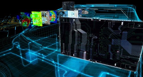
The next step introduces the most significant barrier: going into 3D CAD to evaluate mechanical physics. To manually create a 3D representation of the board layers, copper traces, component locations, holes and housing requires a substantial time commitment. In most cases, this was either not done, or greatly simplified so as to potentially miss important interactions.
While this may be suitable for electronic systems of the past, it will not suffice for the new safety critical requirements of autonomous and electric vehicles and ADAS. One component placed in a high vibration amplitude location will trigger early failure – game over!
Once an automated conversion of 2D circuit board layout to 3D CAD is achieved, the development process can move forward. This includes CAE meshing of CAD model, conjugate thermal analysis (including transient duty cycle power dissipation & resistance heating of copper traces), thermal stress and vibration stress of the board and components – down to the solder joint level. Then a fatigue assessment of the key stress locations to evaluate durability life. This represents a comprehensive assessment of the circuit board physical structure.
The beauty of such a digital PCB development process is that anytime a change is being evaluated to address an issue, the whole system performance can be verified to ensure all objectives are achieved in a timely manner.
For instance, if a new component needs to be assessed to reduce costs, it may have different thermal characteristics that need to quickly be evaluated; this is a common occurrence. Purchasing is tasked with reducing costs in every way, so if they can save a half cent on a resistor, they’ll pursue it. This is often done just before manufacturing, because problems can occur at the last second! So having an integrated circuit board development process as part of a digitalization strategy is critical for many different aspects.
This concludes the third part of our series on electronics systems and the challenges to provide solutions for future autonomous and electric vehicle products. In part four, we will discuss accelerating circuit board layout design through advanced digitalization. If you wish to start from part 1, please click here.
About the author
Greg Roth is the director of automotive and transportation solutions in the Industries Group at Siemens PLM Software. In his current role, he champions CAD, CAE & PLM technologies and processes for companies at a global enterprise level so they can achieve substantial reductions in product development costs and time while improving overall quality. He previously held positions at Ford Motor Company, Eaton Corporation and Amcor Packaging. He was also chief engineer for the CAE and NVH departments at ZF-TRW Automotive North America Braking Systems in Livonia, Michigan. Greg holds an master’s degree in mechanical engineering from the University of Michigan, a master’s degree in electronics and computer controls engineering from Wayne State University and a bachelor’s degree in mechanical engineering from Michigan State University.