Hierarchical DFT on a flat layout design? No problem, says ON Semiconductor
By Vidya Neerkundar – Mentor, A Siemens Business
Design teams are always looking for new ways to perform the more time-consuming DFT tasks more efficiently as the size and complexity of the design increase. Adopting a hierarchical DFT methodology is proving to be a winning strategy for many semiconductor companies.
Moving DFT up in the flow to the RTL level helps to reduce the time it takes to perform DFT insertion, but, not all DFT insertion is performed on RTL. Sometimes DFT logic is inserted into gate-level designs. If the place and route is done on the full chip-level design (as opposed to hierarchically), the DFT work would traditionally also be performed once on the full, flat design. However, for large designs with many memory instances, performing DFT on the chip-level design is not likely to be the most efficient DFT method. ON Semiconductor wanted to use hierarchical DFT but still perform physical implementation on the flat layout. This was the challenge to which they applied the Tessent hierarchical DFT flow.
If you want to hear more about hierarchical DFT flows, visit the International Test Conference in Phoenix on October 28-Nov 2, 2018. There, Vidya Neerkundar and Ron Press will be available to explain their poster presentation, “Effective Testing of Identical Hierarchical Cores”. They cover the upfront design planning required and the optimized compression architecture in the hierarchical core(s) that helps resource utilization at the chip-level.
ON Semiconductor performed a study on the insertion of memory BIST for a multi-million gate-level netlist with 300 memory instances. The physical implementation will be done using a flat layout, but they needed to insert and implement DFT more quickly than what is possible on the flat layout. The time required to insert memory BIST and perform synthesis of the memory BIST hardware typically took ON Semiconductor about 9 hours. The long run times prevented the engineers from performing what-if scenarios to optimize the outcome.

ON Semiconductor divided the multi-million gate-level design into 13 submodules (not physical hierarchical regions) and then performed memory BIST insertion and synthesis on these 13 sub modules in parallel. The time it took to perform both memory BIST insertion and synthesis was drastically reduced, allowing the team to perform multiple iterations within the same day and also finish other tasks that need to be performed, including running what-if scenarios to optimize the results.
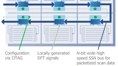
After hierarchical memory BIST insertion and synthesis, the chip-level DFT work included the use of the IJTAG (IEEE 1687 standard) and Tessent MemoryBIST to help generate memory BIST patterns not just for testbench simulation but also for generating WGL/STIL patterns that can be supplied to the tester.
ON Semiconductor operates in a highly competitive IC market, so any easy-to-adopt technique that improves the design time, lowers cost, or improves quality can infer a competitive edge. For DFT engineers, an area ripe for improvement in runtime and quality on huge designs is in DFT insertion and synthesis. Hierarchical DFT allows the DFT work to be performed in concurrent parallel insertion and synthesis runs. As the ON Semiconductor case study shows, hierarchical memory BIST works for even for designs that will go through a flat place and route flow. Tessent MemoryBIST and other Tessent products helped ON Semiconductor to attain the desired results with improved productivity.