Improve IC development and reduce risk for big designs by moving DFT up and left
By Ron Press, Mentor Graphics
Complete all the DFT work weeks earlier than usual by using a hierarchical test strategy. There are many benefits to the divide-and-conquer approach to DFT, as this article explains.
Through generations of technology advances, I’ve seen that as a particular task gets more important and usually more complex, it becomes the target of automation and so becomes greatly simplified.
Sometimes this added automation significantly impacts the design flow causing a shift in the types of specialties and functions engineers perform. With the automation, many of the specialists performing the previous tasks might not be needed in the same numbers. But, the automation capability itself requires new and more complex powerful functions. This is exactly what is happening now with the adoption of hierarchical test methods for large designs.
Complete all the DFT work weeks earlier than usual by using a hierarchical test strategy. There are many benefits to the divide-and-conquer approach to DFT.
It is a common philosophy to break down a large and complicated task into smaller and simpler tasks. IC design follows this principle; a complex project or desired system is broken down into smaller and smaller pieces until each individual part is simple enough with well-defined interfaces that it can be completed stand-alone, without needing to understand the complexity of the overall system.
Scan technology works the same. Instead of dealing with a complex functional device with many sequential states, scan breaks it into many small, simple, mostly combinational parts that are easy to test. These parts are so simple that ATPG software can automatically create the patterns for the user. With automation, the work of the test engineer is greatly simplified. The complex work is automated by ATPG tools such that the user has a higher level and simpler task, thus “shifting up” the user’s work. Similarly, if a large task is broken into smaller pieces then often much of the effort can be done earlier in the flow, or “shifted left.”
In a recent Mentor Graphics industry survey, 40% of companies designing ICs reported that they are building ICs with 50 million gates or more today. In my experience, this is a threshold for where generating DFT and scan patterns can get painful. Trying to perform the majority of the DFT and pattern-generation work on the full design is unnecessarily complex and difficult and has to wait late in the design flow for the full design to be ready. This could result in delayed tape-out schedules, DFT or ATPG surprises late in the design flow, and compromises on test quality.
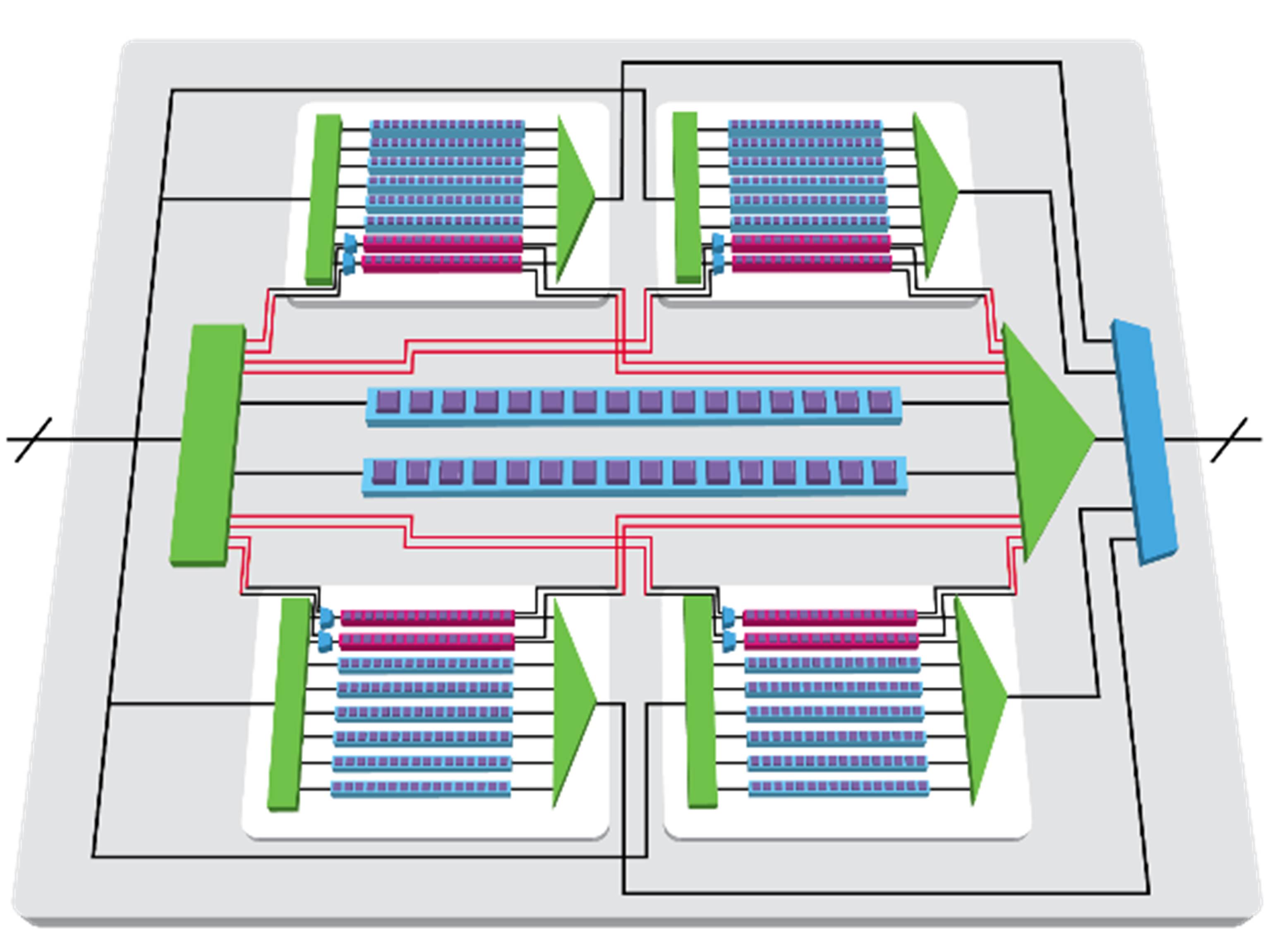
Figure 1. Hierarchical DFT breaking a complex full design into easier-to-manage parts
As one solution, chip makers are turning to hierarchical DFT, illustrated in Figure 1, which lets them break the large design into smaller parts with well-defined interfaces (wrapper chains) such that each part (block) can go through DFT insertion and pattern generation independent of the overall design. Figure 1 shows a hierarchical architecture with scan, embedded compression, and wrapper chains in each block and at the top level. This method removes a huge amount of complexity and greatly simplifies the problems of testing very large designs. In addition, the DFT and ATPG work is shifted left in the design flow and can be completed as soon as an individual block is ready. The patterns created for one block are automatically retargeted/ported and merged if needed with other block patterns in the final design.
With hierarchical test, the complexity of the DFT and ATPG tasks are shifted left so they are earlier in the design cycle. Simulations are also moved left in the flow so they can be completed with the block instead of after tapeout, which often happens but presents a big risk if something fails.
The main feature of hierarchical DFT is completing the pattern generation early at the block level and retargeting/porting and merging the patterns to the top-level design later. This takes the big DFT efforts out of the critical path at the end of the design. The top-level test access mechanism (TAM) insertion to control hierarchical modes is the simple part. Tool automation takes user definitions of which block channels to access at top-level pins and drops in the TAM logic. Retargeting is more than taking block IO values and porting them to the top design. There are many design rules that are constructed and verified in the context of the top-level design to ensure that the block patterns will function properly. Inversions and pipelines in the scan-channel paths between the blocks and top can often occur. Therefore, the ATPG tools are built to automatically recognize inversions and pipelines and adjust the patterns considering them. There is a cost to hierarchical test—adding wrapper chains to isolate each hierarchical block—but it is an accepted tradeoff to enable the work to be done earlier in the flow with much simpler resources.
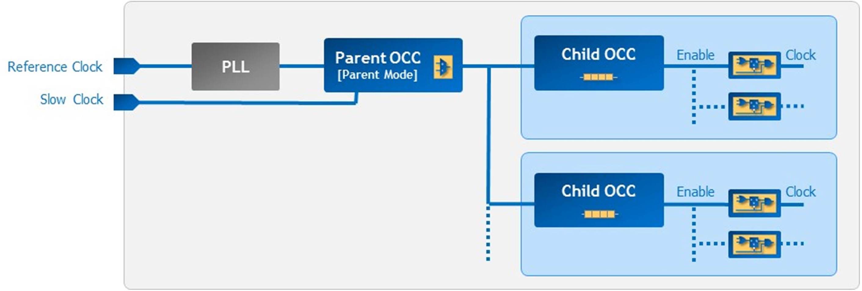
Figure 2. Parent and child OCCs in hierarchical DFT
There are some design techniques that improve the usability of hierarchical test. One is to place on-chip clock controllers (OCCs) within the blocks. This allows programming of the OCCs to be included in the scan data for each block pattern, making it very easy to port to the top level. However, some designs use architecture such as clock mesh and have the OCC at the top level since that clock is broken into many branches by the time it gets into the block. In order to support this architecture, but still include clocking data in each block-level pattern, you can use a parent/child OCC, as shown in Figure 2. The parent OCC can be statically programmed to select the clock to enter the block, but the simple child OCC can be used within the block patterns to control the clock sequences. When top level patterns or patterns at the parent OCC level are generated the parent OCC is configured in a standard mode such that clock sequences are controlled with each pattern.
Because of its considerable benefits, hierarchical DFT is becoming a popular technique for large designs over 50 million gates and is viewed as vital for most very large designs over 100 million gates. Hierarchical DFT requires a little more structure with block scan wrappers and OCC locations but the benefits are huge. It provides a significant value by simplifying the full-chip problem, requiring 10x smaller workstations, and faster ATPG run times. But, what is often the most critical advantage of hierarchical DFT is that the problem is shifted left. I often hear companies state that with hierarchical test they can complete their DFT work weeks earlier.
Author
Ron Press is technical marketing director at Mentor Graphics.

This article was originally published on www.evaluationengineering.com


Comments
Leave a Reply
You must be logged in to post a comment.
Could you explain the pulse point when we use child OCC?
Hi, not sure what you mean by “pulse point”. The easiest case is to just have one or a few OCCs located within the block that will have patterns retargeted. In cases where a main OCC control cannot be conveniently moved within the block (like clock mesh) then parent/child is a good option.