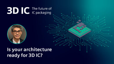
3D IC is here: But is your architecture ready for it?
As 3DIC adoption ramps up, it’s becoming clear: microarchitecture needs a rethink. So how do you design hardware that can survive and thrive in the new era of stacked silicon?
In this episode of the Siemens 3D IC Podcast, host John McMillan speaks with Pratyush Kamal, Director of R&D for 3D IC Solutions Engineering at Siemens Digital Industries. With decades of experience spanning Qualcomm and Google, Pratyush brings deep insight into the evolution of IC design—and how 3D integration is transforming every layer of the design stack.
From redefining how and when microarchitecture decisions are made to overcoming the thermal, testing, and failure analysis challenges that come with 3D stacking, this episode dives into the critical topics design teams need to understand today.
You’ll also hear how AI, automation, and cross-disciplinary expertise are reshaping team roles—and why software-defined silicon is redefining the design process itself.
This episode is essential listening for IC architects, system designers, and packaging engineers navigating the transition to advanced 3D IC platforms.
What You’ll Learn in this Episode:
- What is microarchitecture in IC design? (2:30)
- What does microarchitecture mean in 3D IC design? (3:20)
- How early do we need to consider microarchitecture in 3D IC design? (4:45)
- The main issues system designers face concerning the increasing complexity of microarchitecture (5:50)
- How are roles changing to enable a more holistic outlook on 3D IC microarchitecture? (9:15)
- What would enable non-silo design practice? (11:00)
- Closing thoughts (11:55)

Pratyush Kamal
Pratyush Kamal is director of central engineering solutions at Siemens EDA. Kamal is an experienced SoC and systems architect and silicon technologist providing technical leadership for advanced packaging and new foundry technology programs. Kamal previously held various jobs at Google and Qualcomm as SoC designer, SoC architect, and systems architect. Kamal also led 3D IC research at Qualcomm, focusing on both wafer-on-wafer hybrid bond and monolithic 3D design integrations.
Explore More on 3D IC Innovation & Research
Deepen your understanding of 3D IC design with these resources:
- Home | UCIe Consortium
- Die Stacking (3D) Microarchitecture | IEEE Conference Publication | IEEE Xplore
- Fine grain 3D integration for microarchitecture design through cube packing exploration | IEEE Conference Publication | IEEE Xplore
- Opportunities, Challenges and Mitigations in 3DIC Design, Test, and Analyses | IEEE Conference Publication | IEEE Xplore
- Design-Aware Partitioning-Based 3-D IC Design Flow With 2-D Commercial Tools | IEEE Journals & Magazine | IEEE Xplore
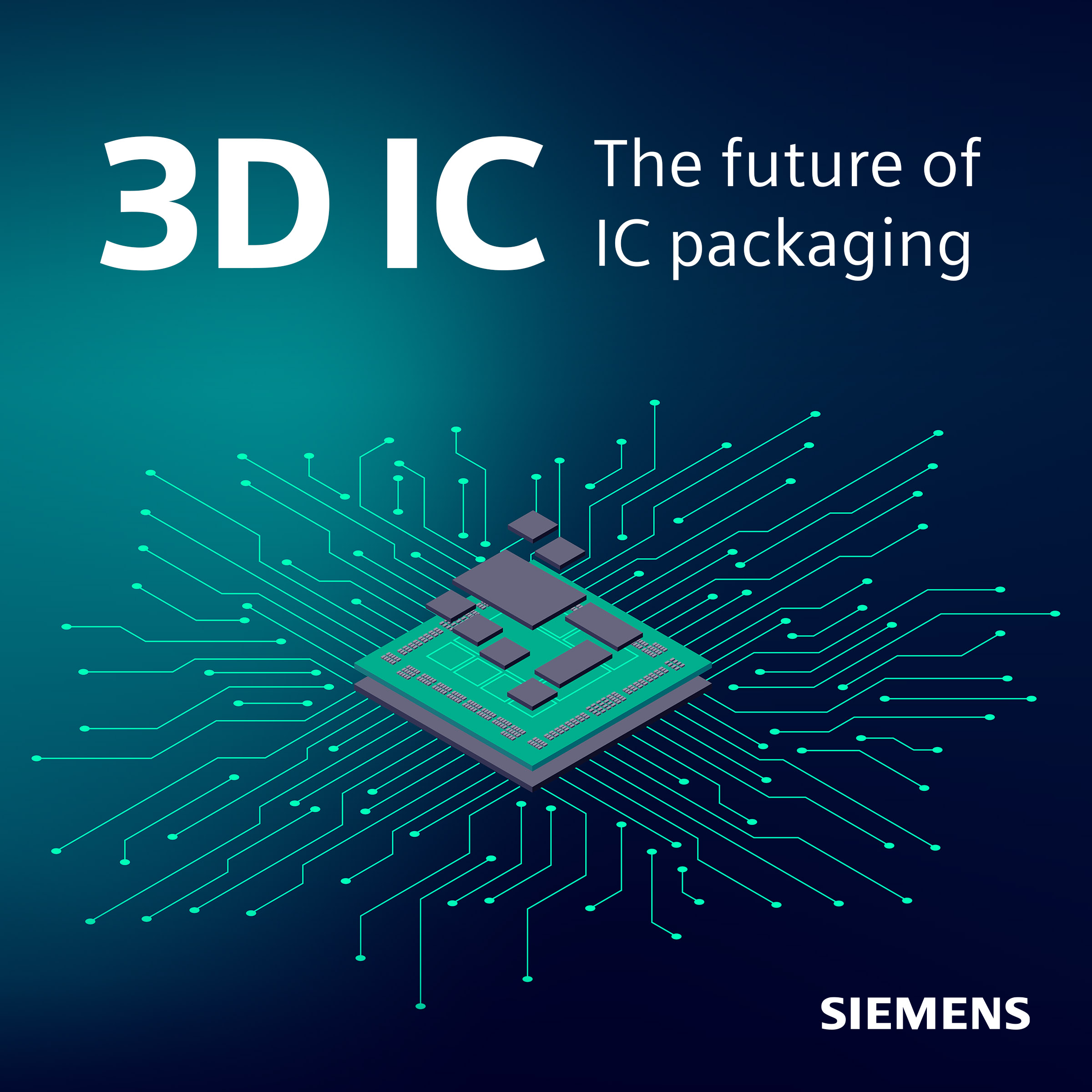
3D IC
3D IC is the future of IC packaging. Learn with us how to prepare for it.
