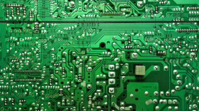
EMI problems are easier to fix than you might think
Many electromagnetic interference (EMI) problems on PCBs happen when antennas are unintentionally created on the board. How can this be avoided? By making sure currents, especially high-frequency currents, travel in a loop. On high-speed lines, that loop is made up of a PCB trace AND the reference plane below it. Put a break in either one, and you’ve created an antenna. Obviously you would never consider breaking a signal trace, so why have a break in its reference plane?
I discuss this in greater detail in a recent article in Printed Circuit Design and Fabrication Magazine: http://pcdandf.com/cms/component/content/article/246-2012-articles/9315-pcb-design
Avoiding such cases on very complicated designs with low layer counts requires some planning early in the design cycle. Different busses should have their layers pre-determined and should be routed adjacent to ground and/or their associated voltage planes. Otherwise, a trace could get routed across a plane split, which is a break in the reference plane that can cause EMI issues. Even with careful planning, signals may still end up getting routed across splits. Or, large gaps in the reference plane may get created from neighboring antipads or other similar structures. These issues can quickly and easily be pinpointed with an electrical rule checker like HyperLynx DRC (http://www.mentor.com/products/pcb-system-design/circuit-simulation/hyperlynx-drc-emi-emc), and the issues resolved before the board gets fabricated. Trying to fix these kinds of issues on a fabricated board in the lab is next to impossible.


