Facing a New Age of IC Design Challenges Part 1
In an industry accustomed to incremental change, Veloce CS is a departure because it is a complete three-in-one system, a development that Ron Wilson, a longtime technology editor, explores with Brunet in this 2-part blog.
Wilson: How do you describe the Veloce CS system?
Brunet: The Veloce CS system is architected for congruency, speed and modularity and supports design sizes from 40-million gates to designs integrating more than 40+ billion gates. It executes full system workloads with elevated visibility and congruency, enabling teams to select the right tool for a task’s unique requirements for faster time to project completion and decreased cost per verification cycle.
Wilson: Why now?
Brunet: We recognized the discontinuity triggered by the convergence of AI-related hardware, software defined product, new process technology and the emergence of chiplet-based systems. We responded by developing three economical, scalable systems that directly address the needs of design teams. Our goal with the Veloce CS system is to be the instrument to create the next-generation advanced ICs and multi-die modules bringing new levels of productivity to design teams and new levels design and schedule integrity. We envision a new value proposition for IC vendors, IP houses or systems developers who will transform these advanced IC designs into earnings growth.
Wilson: What has changed to make it possible to improve the value proposition?
Brunet: Major changes in design scale, the role of software, the physical environment where chips are designed and the technology that underlies the Veloce CS system.
The scale of IC designs has increased, driven by demands for a few key applications: datacenter CPUs and GPUs and AI accelerators. In the latter case, exploding demands of training for generative AI models and the research into GenAI show an insatiable appetite for hardware.
Chip designs now encompass the equivalent of tens of billions of gates. The industry responded with new 3 nm and 2 nm process generations and multi-die modules. Design teams want to treat the RTL for these dies as a single monolithic chip pushing equivalent gate counts beyond the reach of a single 2 nm die.
Meanwhile, size and complexity of software stacks grew faster than hardware because of who is creating the designs. Until recently, CPUs and GPUs, designed by merchant semiconductor companies or IP houses, passed elaborate verification suites to prove they correctly implemented an instruction set architecture or command set. Above that level, software stacks—drivers, operating systems, middleware and especially application code—were the purchaser’s problem.
Many of today’s ICs are designed by systems houses—cloud service providers, telecom giants, automotive manufacturers, aerospace companies—for specific applications and are not the product. The system, including the full software stack, is the product that a design team must verify. It is no longer sufficient to check the RTL design with synthetic benchmarks and fragments of hardware-dependent code. Design teams now verify and characterize a system design beginning at RTL running full production workloads. This need has shifted the center of effort in front-end design from verifying the RTL against a specification to proving the RTL under full software stacks including application code.
The two branches of development—RTL for hardware and software for the application—must proceed in parallel. Early in the design, most of the effort will be software design and debug with two-way communications between the RTL and software teams.
Wilson: Why three systems?
Brunet: RTL designers, software coders and system-level engineers must collaborate. As the RTL design team is creating and verifying the chip design, software teams are developing and testing driver, operating-system, middleware, and application code and integrating it with the chip design and the board-level hardware. Design is underway on boards and peripheral devices for the larger system.
These tasks proceed concurrently, and one system cannot optimally meet all three of these needs. It takes three to meet the stringent requirements to support today’s designs and all three must share much of their DNA.

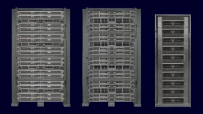
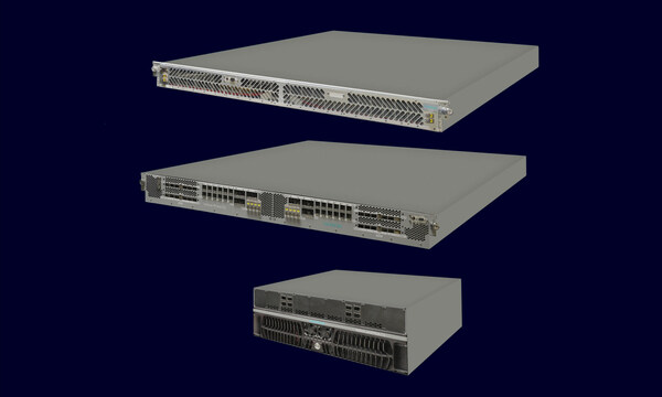
Jean-Marie Brunet is Siemens EDA’s Vice President and General Manager of Hardware-Assisted Verification (HAV). He and his group recently announced the Veloce CS hardware-assisted verification and validation system including Veloce Strato CS, an emulation system; Veloce Primo CS, an enterprise-scale prototyping system, and Veloce proFPGA CS, an at-speed prototyping system.