Why adopt an integrated toolchain for advanced package design?

Growing complexity in high-density advanced packaging requires a toolchain to reduce exponentially increasing design overhead
One seamless solution from start to finish:
- Use one toolchain for design, simulation, and test
- Implement a standardized data format to enable seamless tool to tool exchanges
Across the semiconductor industry, it is becoming increasingly apparent that there is a need for better communication between the ECAD and MCAD domains. Most companies recognize that this communication gap hinders time to market, restricts profit margins and significantly impacts quality. But any workable solution must also fully address the many complex challenges that package designers face in collaborating across domains to provide the most cost-effective, innovative and reliable electro-mechanical designs essential in today’s competitive market.
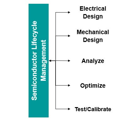
Electrical computer-aided design (ECAD) – Mechanical computer-aided design (MCAD)
- ECAD-MCAD to simulation (electrical, thermal, and mechanical)
- Develop integrated circuits faster through an integrated ECAD-MCAD-simulation ecosystem.
One of the most critical challenges in advanced packaging is keeping semiconductor temperatures at bay. This is why thermal design has become an increasingly important component of the package design workflow. By keeping the junction temperatures low, issues such as cracks or delamination in the die attach layer or in the C4 bumps are simply avoided.
The thermal and mechanical behavior of complex package structures should be analyzed using co-simulation of dedicated CFD and FEA solvers. We’d like to illustrate how easy this process can be in a few simple steps that follow.
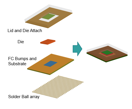
The package definition can come from an MCAD tool or be created directly within a thermal simulator. We used Simcenter FLOEFD as a CFD solution embedded in the MCAD NX environment to create the package definition below. Since FLOEFD has a ‘Package Creator’ tool that supports the quick modeling of common package types using a parameterized input, a model of an FCBGA (Flip Chip Ball Grid Array) Package can be created this way in minutes. See Figure 1.
Built on a foundation of intelligent, fast and accurate technology, Simcenter FLOEFD helps reduce the overall simulation time by as much as 75% and enhances productivity by up to 40x.
The component can be simulated individually or mounted on a PCB resembling its intended application. This is why Siemens supports seamless PCB model import from Xpedition to the MCAD NX environment, where the modeled chip is added with all its internal details. See Figure 2 below.

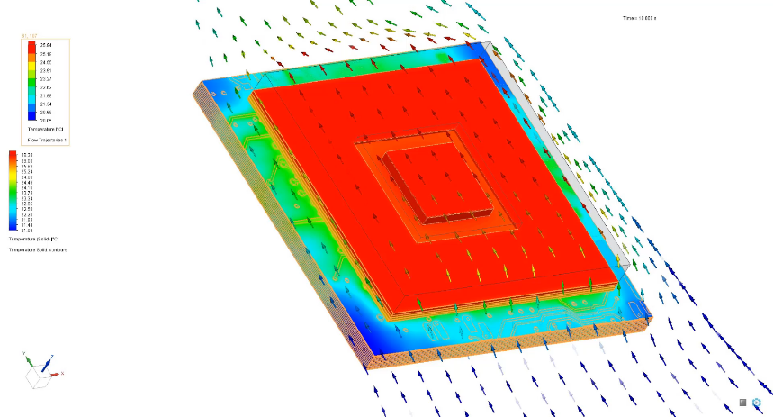
The next step is to perform simulation using the entire PCB or a narrow cut-out section below the package, depending on the study goal. Before the thermal simulation begins, the material definitions should be adjusted and imported directly from the Package Creator or added manually. The model can be conduction only, or convection and radiation can be enabled. A refined thermal mesh is created automatically in FLOEFD, then the simulation can begin. This current example had 1.2 Million cells generated in under two minutes and took 25 minutes to reach a solution for a transient simulation, far outpacing conventional methods. Results can be seen below, including material temperatures and airflow over the device.
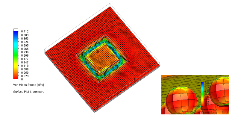
Simcenter FLOEFD can create an efficient hex-dominant mesh and conduct linear stress analysis directly using the existing model and calculate fields such as the Von Mises stress or equivalent tensile stress without leaving the tool:
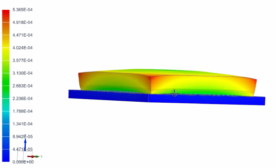
To perform non-linear analysis, the model is transferred to Simcenter 3D without leaving the MCAD NX ecosystem. Mesh, materials, glue contacts, constraints, and loads (constant values or transferred from another Simcenter FLOEFD calculation) can be transferred to Simcenter 3D seamlessly, where you can choose from various useful solvers, such as creep, displacement, and fatigue simulations for thermal cycles. Figure 5 shows creep simulation results of our example case for thermal load.
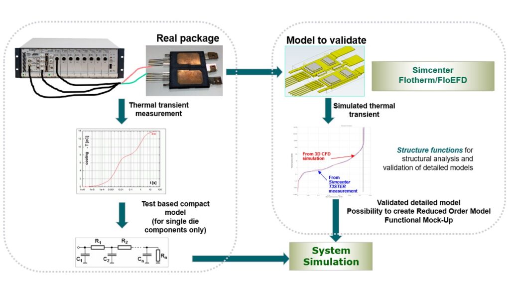
Your simulation results will only be as good as its import parameters. Even in the most carefully prepared models, it is recommended to test the resulting thermal properties of a component and if a mismatch between simulation and test results, the thermal model parameters should be re-calibrated. Siemens offers a unique test approach called Simcenter T3Ster (Thermal Transient Tester), which can apply a power step on the semiconductor die and measure its corresponding thermal response. The ‘unit power step response’ will be characteristic of the thermal system, so the transfer function of the package can easily be calculated.

As a result, the package can be modeled with an equivalent thermal R-C network consisting of hundreds of elements. For essentially 1-D heat spreading cases, these R-C elements strongly correlate with the real thermal properties of the individual structural layers of the package.
For model calibration purposes, if we replicate the test within Simcenter FLOEFD, using the same boundary conditions, input power and transient time steps as in the test, the R-C network model describing the digital twin of the package must be the same as the R-C network model obtained from the test. In case of a mismatch, Simcenter FLOEFD can automatically find the missing contact thermal resistance values, adjust the ill-defined thermal conductivities or even adjust the geometries if needed.
The calibrated digital twin will have several benefits:
- It will behave thermally exactly like the real physical device, even for transient simulation cases
- The corresponding structural simulations will be more accurate, too, as they need accurate thermal fields as an input
- The behavior of selected materials will be understood and can be saved in libraries and used to create better models
In conclusion, Siemens is the only solution provider to offer an end-to-end toolchain that allows designers to move seamlessly through the design process and address growing complexities related to high-density advanced packaging.
Join us at Realize LIVE in Las Vegas, May 9-12, 2022, for our session presentation on Package Design, plus an informative round table discussion. Secure your Discounted Pass – Register Today!
Stay tuned for more insights coming in our next blog post.
Andras Vass-Varnai, Tim Brodovsky, Ramana Kappagantu, and Nigel Richardson also contributed to this article.


