ABCs of PCBs – J for Jitter
Welcome to ABCs of PCBs – a blog series to help new engineers learn about the world of Printed Circuit Boards. I’ll be covering topics from general engineering concepts to PCB design specific rules. As this is a ‘basics’ blog, I’ll keep the content software independent, but any visuals will be from the Mentor PADS Professional PCB suite.
If you missed the last post in this series: ABCs of PCBs – I is for I (Current) click here!
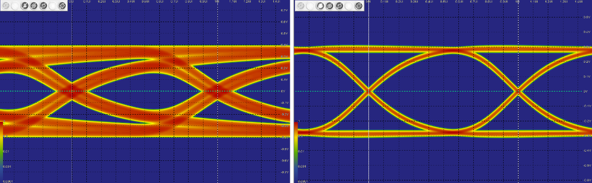
Let’s talk about jitter. No, not the nervous behavior we exhibit or the shaky feeling we get with multiple cups of coffee. In the PCB and electronics world, jitter refers to timing errors.
Jitter can be seen as the variation in a signal from cycle to cycle. It differs from what is expected of the system, usually caused by issues like crosstalk, electromagnetic interference, thermal factors, power noise, or reflections.
There are a few different types of jitter and terminology that you might encounter and you may want to be aware of:
Period jitter
Period Jitter refers to the deviation of an ideal clock period to the actual clock period. It’s typically used to measure jitter in low frequency application. Jitter can occur in every system, so it’s important to check for any faults in the period of clock signals – regardless of speed.
Cycle to cycle jitter
If you take a look at the deviation of a clock edge from its ideal location, you can calculate Clock Jitter. This is extremely important in the timing of a system and can severely affect your final product if overlooked. We’re in an age where the systems have increasing data rates, so timing is everything.
Once jitter is addressed, now you need to find a solution to minimize it. There are many factors to review when limiting jitter, including:
Reviewing the stackup
If it’s a 2+ layer board, you’ll want to make sure signal layers are routed in the middle while the outer layers (top and bottom) are reserved for an option of poured copper, like power and ground, to help with noise reduction. Adding grounding planes can help as well. You can refer to G for Ground Planes to more ideas on how to limit signal interfere with grounding.
Rerouting traces
PCB traces act like transmission lines and can create crosstalk in the signal. Impedance matching, along with proper routing techniques, can limit crosstalk in your designs and directly impacts jitter variations.
Take some time during the PCB design process to consider the factors like crosstalk and power noise that can lead to jitter. You don’t want CPUs to overload, output signals to be distorted, or timing issues to lead to your design’s failure.
Thanks for reading and see you next time for more on the ABCs of PCBs.
-Shivani Joshi