How to reduce time spent placing components, routing traces, and creating planes.
Over my 25+ years of designing PCB’s I’ve always been driven to make the job of designing a PCB as simple as possible. Well over half of those years was spent working as an independent consultant. Every design I was contracted to complete I wanted to finish in the least amount of time so I could move on to the next project maximizing monthly income. As such, I made sure to keep up on the latest technology available in the EDA tool I was using.
Over the years I was able to adapt my designing style for each phase of design like creating library parts, placing components, routing, creating plane areas, and creating documentation based on new technology. The greatest improvement came from routing automation.

I’m not talking about push-button autorouting. I was never a fan of batch autorouting, just like most designers in the industry. I’m talking about interactive routing and autorouting. Using my skills as a designer to guide traces to the proper location and letting the tool do the dirty work of moving objects around to complete traces.
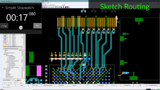
In the images above you can see that with modern Sketch routing technology the time savings is 5X’s faster than interactive routing and emulates both the quality and control of manual routing.
To learn more about Sketch routing technology along with seeing many more layout features and capabilities that you may be missing out on, join our upcoming webinar where I’ll be demonstrating many modern design saving processes and functionality that will definitely reduce design time during your next project. To try this technology for yourself start a Free trial or talk to a PADS Professional expert today.