PCB Design Then and Now
It’s hard to believe that nearly three decades have past since I designed my first printed circuit boards. I can still recall how impressed I was with the first CAD system I’d operated. It was in a futuristic ambient-lit computer room where six or so minicomputer based Calma Systems were installed.
Each Calma workstation included a digital read-out of x-y coordinates illuminated in red located in the upper right corner of the huge digitizer table. Each station also included a console complete with mechanical keyboard and green monochrome CRT’s.
This image 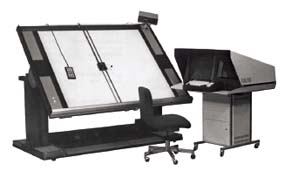 (courtesy of David Weisberg) gives you an idea of the floor space taken-up by the Calma system. A separate “computer room” complete with a raised floor hiding all the AC ducts and cabling housed all the data storage systems that served and backed-up the workstations. There was also a huge HP plotter used to print out each layer of digitized routes that would eventually be scaled and photographed on to clear film in the lab located across the hall. Sound familiar?
You don’t have to have been in the PCB industry for decades to see the evolution of EDA tools for PCB design. The industry has come a long, long way from hand-taping designs and digitizing hand-drawn layers as done with the Calma systems that we literally used to build rooms around. We now use powerful desktop tools installed on laptops and carry them around in backpacks that “usually” fit neatly under the seat in front of you on an airplane.
PCB designers’ responsibilities have evolved proportionally over the decades. A design flow where individuals may have been solely responsible for the schematic or just symbol creation or only the layout of the design without any involvement with other individual tasks in the design flow are long gone.
Today, we must consider every aspect of the design throughout the entire flow. That is, interest in every component, every layer, every trace and every via. We consider signal integrity, we simulate and we validate. We know where the PCB is installed and design with EMI and thermal influences in mind. We collaborate directly with mechanical CAD tools and we analyze completed designs utilizing DFMA tools developed to ensure first-pass manufacturing success.
“PCB design, the methodology of the past, has become the entry point to the wonderful new world of System Design Automation (SDA). PCB itself is being teamed-up with MCM design; 2D, 2 & ½D design, and 3D design; MEMS Design and Mechanical Design. This is giving Mentor and Cadence a door to the future.” (Source: 2014 Marketing Trends: Executive Sumary – Gary Smith EDA. ~ We are left with heavy hearts upon learning that Gary had passed away over the July 4th weekend – he was a true leader and visionary in the EDA industry. We extend our deepest condolences to his family.~)
PCB designers now have the capability and in many cases the responsibility to perform much if not every aspect of the design flow. PADS solutions: Standard, Standard-Plus and Professional are specifically tailored to suit the needs of today’s designers no matter the level of responsibility. Appropriately bundled and proportionally priced to fit your budget.
PADS Standard is geared toward the engineer looking for high value, production proven tools. It provides schematic design and layout capabilities in an intuitive and easy-to-use environment. PADS Standard is ideal for less complex board design where cost is a high priority. Try it now http://www.pads.com/standard/try
PADS Standard Plus is packaged to empower the independent engineer who requires a more complete design flow that includes advanced tool-sets. It has everything that Standard has, plus it is equipped with the enhanced layout and integrated analysis and verification functionality needed to produce quality PCBs, fast. Try it now http://www.pads.com/standard/try
PADS Professional is the most powerful solution, packing all the technology required to accomplish the most demanding and complex designs at an unbelievable price. Professional provides the independent engineer with the technology required to accomplish the most demanding and complex designs. The full flow of PADS Professional lets you design, validate and manufacture PCB-centric systems including advanced FPGA devices. Try it now http://www.pads.com/professional/try
Click image below to compare to PADS products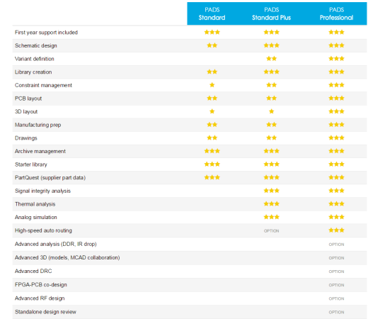 PADS solutions are appropriately bundled to fit your level of design complexity and your budget to ensure that you maintain your competitive edge.
Thanks for reading, John