Behind the Design: Alcatel-Lucent
This is the first in a series showcasing the winners of the 2014 Technology Leadership Awards.
The votes are in for the 2014 TLAs! Congratulations to the 2014 Technology Leadership Award winners! Started in 1988, this program is the longest running competition of its kind in the electronic design automation (EDA) industry. The competition recognizes engineers and designers who use innovative methods and design tools to address today’s complex PCB systems design challenges and produce industry-leading products.
Overall 2014 Winner: Alcatel-Lucent, Italy
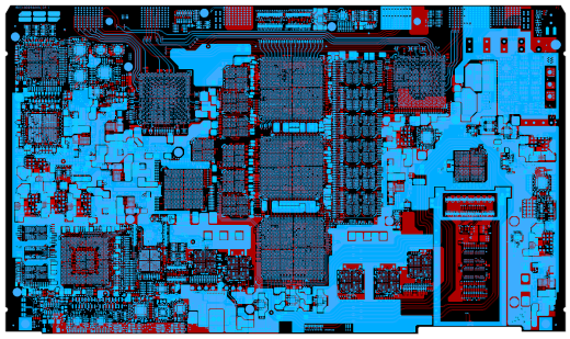
Design: An evolution in core packet processing technology, Alcatel-Lucent’s 1X100GE packet module includes 100Gb/s of total processing power and signals operating at 6/12/28GHz.
Design team: Fabrizio Crippa, Giovanni Villa, Sergio Pirovano, Massimo Pollastri, Stefano Cornini, Luigi Aldeghi, Fabio Villa, Paolo Scotti, Massimiliano Severi, Ivan Malaspina, Fabio Frigerio, and Donato Maggi
Design challenges:
- Design for: signal/power integrity, reliability, manufacturability, cost, and variants
- 6,000+ components, 22,000+ connections, 20,000+ vias, 24 layers
- 70% nets high-speed: used Constraint Manager for more than 200 buses with length controls on ~5,000 nets and more than 10,000 connections; all routed by hand and verified
- Cost constraints for high-volume product drove the overall design process and influenced many of the decisions; limited use of HDI due to cost constraints resulted in greater placement and routing effort
- Placement restrictions: height constraints based on racking system forced all tall comps to one side; couldn’t be over internal high-frequency signals; also had to consider DFM issues associated with rework and testing (100% test point coverage)
- Multi-discipline concurrent design: the board design involved several disciplines including signal and power integrity, mechanical, thermal, layout, and DFM/DFT. To achieve the aggressive schedule, each of these components was implemented in parallel with the design team sharing data at appropriate stages. The design team used the flexibility of their Xpedition® tool chain to collaborate in real time during schematic entry, layout, and manufacturing validation.
- “But the biggest challenge was to make sure that this project works the first time, and this has been met!”
Design tools:
- Xpedition Enterprise flow
- Many power supplies with currents higher than 30Amps and tight drop voltage tolerances required detailed study and simulation with HyperLynx® PI. Power integrity analysis performed by HyperLynx in early and final design stage allowed PI expert to verify if the two distinct facets of PCB power integrity (DC and AC) respect the design specification, suggesting updates where needed as part of the cost reduction strategy.
- Thermal analysis used to determine the exact size of heat sinks to ensure operation within the required temperature range. FloTHERM was used to simulate the thermal profile of each sensitive component, at PCB and complete systems level, especially during the preliminary phase of the design process to keep each device in the operating temperature range improving the PCB′s thermal reliability with the goal to reduce possible PCB re-spins due to thermal issues.
- Signal integrity (HyperLynx SI) was used in the first stage of the project to characterize the critical HF signals. Each significant frequency type was simulated and recorded. When multiple drivers could be selected for a specific device, the full range of driver to receiver simulations were performed so that the overall design performance could be determined. These results were used to define the constraints for the board but the long term goal is to provide a database of response characteristics so that they can be used by engineers on future design work.
- Xtreme design technology was utilized so that more PCB designers could work at the same time on the single database without work divisions or merge operations, keeping the constraints intact.
- DFM verification by Valor NPI during the design process made it possible quickly send feedback to the PCB designer for updates or improvements before releasing the final database. This helped improve manufacturability and product quality.
Comments from the Judges:
- “One serious board design!”
- “They did a great job at describing the issues they face in the design. This is a high volume board that had to not only resolve the high level of signal speeds, current, and high pin count BGA’s, but address field repair and total cost reduction the first time out.“


