Products
NASA Wins Mentor Technology Leadership Award With PADS!
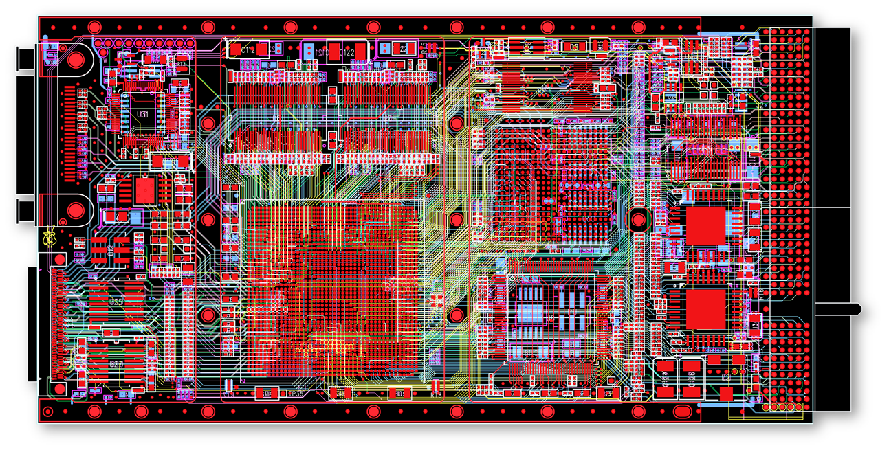
![]() Congratulations to NASA Goddard Space Flight Center, United States
Congratulations to NASA Goddard Space Flight Center, United States
Category: Military & Aerospace – End Product: Spacecube Processor
DESIGN TEAM: Dave Petrick, D.Albaijes, Banks Walker

This design is used in a multitude of applications for solving complex science data processing requirements as well as those that require a radiation hardened and reliable solution, including space systems.
Design goals and challenges:
- To improve performance by 10-100X over ‘state of the art’ space flight processors while lowering power consumption, size, cost.
- Most complex components on the board were back-to-back FPGAs which drove the stackup-up, via architecture, routing, signal integrity, power integrity, thermal design, structural design, and manufacturing requirements of the board design.
- 4 voltage rails with tight tolerances drove the layer stackup and PDN design (mirrored)
- First board manufactured with via-in-pad for a high-pitch column grid array. This was necessary to achieve fan-outs with 1mm pitch BGA’s. This was also required to achieve IPC quality certification and meet reliability requirements.
- Multiple high-speed I/O protocols required extensive pre/post layout SI analysis
- Tradeoff studies:
-Stack-up: Routability (CGA fan-out) vs. manufacturability/reliabilty vs.
PDN & SI performance
-Placement (Dense design, need to leave room for vias, mechanical devices, etc. )
- Design for space environment: thermal analysis to validate conduction to baseplate and placement of high-power components; required extra stiffening for back-to-back components; rad-hard components and circuitry
- Right-first-time: Eliminate manufacturing re-spins by analyzing and correcting problems throughout the design process.
- Signal integrity analysis (pre- and post-route) was used to perform placement studies to arrive at solution to fit all of the components. Easily able to add layers based on design changes.
- ICX and HyperLynx LineSim (pre and post route) were used to eliminate/optimize termination schemes in order to free up board area real estate and routing resources.
- Used HyperLynx stack-up editor to validate manufacturer-provided material parameters
- Power integrity analysis was required to ensure that the power distribution net (PDN) design would meet the electrical requirements on each of the voltage planes from DC to high frequency. The analysis was critical to the design process as it provided a means to identify and correct power distribution problems prior to manufacturing.
- Performed IBIS-AMI channel analysis to validate 3Gbps data rate without having to back-drill vias (lowered mfg costs, accelerated delivery schedule)
- Modeled multi-board scenario to ensure electrical specs could be met.
Be sure to check out all of this year’s winning design teams and see the electronics industry’s most leading-edge designs here: 2014 Technology Leadership Awards
Congratulations to all!
John